株式会社")
グローバルセミコンダクター 梱包 メーカー. the パッケージ基板 昭和電工と味の素のハイス材を使用.
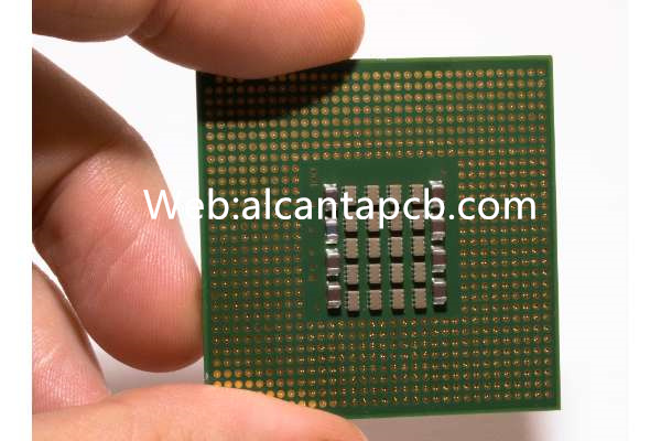
チップやその他の部品を運ぶのに重要な役割を果たします, 電子機器に安定性と接続性を提供する. 半導体メーカーは、製品の性能と信頼性に直接影響を与えるため、パッケージ基板を優先します。. チップをサポートして接続するだけではありません, 回路基板としても機能します, コンポーネント間で信号と電力を伝送することにより、電子機器の適切な動作を保証します。. 建物の基礎に相当する, パッケージ基板の強度が最も重要です; 侵害された場合, デバイス全体の安定性が損なわれます. したがって, メーカーは、今日の競争の激しい市場環境において製品の競争力とユーザーの信頼を維持するために、高品質のパッケージ基板の設計と製造に細心の注意を払っています。.
パッケージ基板の種類は何ですか?
現代のエレクトロニクス産業では, パッケージ基板技術は、半導体パッケージングメーカーにとって極めて重要な注力分野として際立っています。. さまざまなタイプのパッケージ基板が電子デバイスの多様な要件に応えるだけでなく、独自の特性と適切な用途を発揮します。.
HDIボード, 高密度配線技術の例, 精密な製造プロセスにより、限られたスペース内により多くの接続を収容できる能力が特徴です。. これらのボード, 世界的な半導体パッケージングメーカーが提供, いくつかの重要な特性を紹介する:
高密度: 多層スタッキング設計を採用, HDI ボードにより、より小さな設置面積でより多くの接続ポイントを実現できます。, 高密度な配線と部品配置が可能.
高性能:よりコンパクトな接続で, HDI ボードは優れた信号整合性と電気的性能を実現します, 高品質の信号伝送が要求されるアプリケーションに最適です。.
応用: 携帯電話などの小型電子機器に広く採用されています。, 錠剤, そしてラップトップ, HDI ボードは、より合理化された軽量設計を実現する上で重要な役割を果たします。.
堅牢な統合:リジッドボードとフレキシブルボードの長所を組み合わせる, リジッドフレックスボードは独特の形状や曲げのニーズに対応します, 設計の柔軟性と信頼性の向上.
スペースの最適化:スペースを有効活用したデザイン, リジッドフレックスボードによりコンパクトなレイアウトを実現, スペースを節約し、厳しいサイズ制約のあるシナリオに対応します.
適用範囲:自動車エレクトロニクス分野で広く採用されています, 医療機器, 航空宇宙, その他の分野, リジッドフレックスボードは大型サイズの要件に対応します, 重さ, と信頼性.
HDI およびリジッドフレックス ボードを超えて, 半導体パッケージングメーカーは、他にもさまざまなタイプのパッケージ基板を提供しています, 標準両面基板を含む, 多層基板, などなど. それぞれのタイプは、電子機器の多様なニーズやアプリケーション要件に合わせた特有の特性を備えています。.
パッケージ基板を選ぶ理由?
今日のテクノロジー業界では, パッケージ基板は、その卓越した性能上の利点により、世界の半導体パッケージング メーカーの間で好まれる選択肢として際立っています。. 従来のボードと比較して, 密度に優れたパッケージ基板, シグナルインテグリティ, そして耐久性. その設計により、より高いコンポーネント密度が可能になります, 電子製品により多くの機能モジュールをより小さなフォームファクターに統合できるようにする, スリムさの要求に応えます, 軽さ, 現代のエレクトロニクスにおける小型化. さらに, 優れた信号伝送性能を実現するパッケージ基板, 信号損失と干渉を低減することで電子機器の安定性と信頼性を確保, それにより製品のパフォーマンスレベルが向上します. さらに, 耐久性に定評のあるパッケージ基板, 過酷な環境下でも安定した動作を維持できる, これにより、電子製品の寿命と信頼性に対する確実な保証が提供されます。.
第二に, コストパフォーマンスに優れたパッケージ基板. 製造工程中, パッケージ基板の高度に統合され最適化された設計により、材料費と人件費を削減し、生産効率を向上させることができます. 加えて, パッケージ基板の設計により、より高い回路密度と機能集積を実現できるためです。, 電子製品の全体的なコストを削減できる. これらのコスト上の利点により、パッケージ基板は多くの電子製品メーカーにとって第一の選択肢となっています。, 特に激しい市場競争とコスト圧力に直面して, その価値はさらに重要です.
パッケージ基板は、高度な製造プロセスと技術により、比類のない設計と製造の柔軟性を提供します. これにより、メーカーは顧客の固有の要件に合わせて製品を正確に調整できるようになります。, パーソナライズされたソリューションが得られる. この適応性により、さまざまな業界やアプリケーションにわたってパッケージ基板に明確な競争力がもたらされます。, 顧客の多様なニーズに効果的に対応できるため、, 電子製品の革新と進歩を促進する.
要約すれば, 世界の半導体パッケージングメーカーは、その卓越した性能によりパッケージ基板を選択しています, 費用対効果, 多彩な設計と生産能力. これらの特性により、パッケージ基板はエレクトロニクス業界において極めて重要な技術として位置づけられています。, エレクトロニクス製品の開発と進化の基盤となる.
パッケージ基板の製造工程とは?
設計フェーズ: パッケージ基板を作る最初のステップは、パッケージ基板を設計することです. この段階では、製品の特定のニーズと仕様が考慮されます。, サイズも含めて, 階層, 配線, 等. 設計チームは設計図を作成するために CAD ソフトウェアを使用することがよくあります。.
材料の準備: 次は材料の準備段階です. この段階では, マザーボードと基板の製造に使用される基板とラミネート材料を準備する必要があります. これらの材料には通常、グラスファイバーが含まれます, エポキシ, 等.
プリント基板の製造 (マザーボード): 初め, メーカーがマザーボードを用意します. これには、特定のサイズの銅箔の上にグラスファイバーの布を置き、フォトリソグラフィーを使用してその表面に導体のパターンを作成することが含まれます。.
パッケージ基板の製造にはいくつかの重要なステップが含まれます. 最初は, メーカーは材料を準備し、基板レイアウトを設計します. その後, マザーボードと基板を別々に生産している, これには、ラミネート層と導体層を積層して、必要な構造と接続特性を作成する必要があります。. これに続いて, マザーボードと基板は接着剤を使用して接着されており、堅牢な接続が実現されています。. さらに, 特定の顧客の要件を満たすために、金メッキや穴あけなどの他のさまざまなプロセスを実行することもできます. 全体, 製造プロセスでは、最終製品の品質と性能が顧客の期待に沿っていることを保証するための精度と技術的専門知識が必要です。.
パッケージ基板はどのような分野に適用されますか?
パッケージ基板技術は、多くの業界の半導体パッケージングに不可欠です, 電気通信を含む, 健康管理, 自動車, その他. 電子機器の安定した基盤として機能します。, パフォーマンスと機能の向上を可能にする.
電気通信分野内, パッケージ基板は、基地局などのさまざまな通信機器の製造に幅広く使用されています。, ルーター, および光ファイバ伝送装置. 高密度・高速伝送能力を活かして, データ転送速度の高速化が可能になり、より信頼性の高い信号伝送が保証されます。, したがって、ネットワークパフォーマンスとユーザーエクスペリエンスが向上します.
医療分野内, パッケージ基板は、画像装置や監視装置など、数多くの医療機器に応用されています。. 安定性と信頼性により、正確なデータ収集と送信が可能になります。, 最終的には医療従事者に正確な診断情報を提供する, これにより、医療サービスの質と効率が向上します。.
パッケージ基板技術は自動車産業において重要な役割を果たしています, 車内の電子システムに不可欠なサポートを提供する. 車載エンターテイメント システムの機能を有効にします。, 運転支援機能, などなど, 自動車の過酷な環境で一般的な高温および高圧に対する耐性を提供することにより、. この技術は、車載電子機器の安定した動作を確保し、乗員の安全性と快適性の両方を向上させます。. さらに, パッケージ基板技術は自動車用途に限定されず、その重要性は通信や医療などの分野にも広がります。. 電子機器の性能や機能を強化することで, さまざまな領域の進歩と革新に貢献します, それにより社会の進歩において極めて重要な役割を果たします.
パッケージ基板を取得する方法?
パッケージ基板を入手したい方へ, 世界的な半導体パッケージングメーカーまたはその正規代理店とつながる手段がいくつかあります。. 当社は、お客様が必要とするパッケージ基板を入手できるよう、次のガイダンスを提供することでお手伝いいたします。.
パッケージ基板に関する情報にアクセスするには, 信頼できる世界的な半導体パッケージング メーカーやその正規代理店などのオンライン リソースを利用できます。. これらの企業は通常、詳細な製品情報を提供します。, 連絡先の詳細, 公式ウェブサイトから問い合わせるオプション. オンライン プラットフォームを探索することで, さまざまなパッケージ基板の種類について学ぶことができます, 仕様, 価格の詳細, 注文手順, およびその他の関連情報が提供されます.
さらに, 業界展示会に参加することでパッケージ基板に関する情報を収集できます, 博覧会, または技術カンファレンス. 半導体メーカーが集まるイベント, サプライヤー, 世界中の専門家と. これらの集まりで彼らと直接関わることで、直接コミュニケーションが可能になり、パッケージ基板の最新の開発や技術進歩について常に最新情報を得る機会が得られます。.
加えて, パートナーとの接続を確立することもできます, 他の業界に関連するサプライヤーまたは技術コンサルタントがアドバイスや推奨事項を求める場合. より専門的なサービスとサポートを提供するために、信頼できる世界的な半導体パッケージング メーカーまたはその認定ディーラーを推奨する場合があります。.
パッケージ基板に関するあらゆるニーズについては、お気軽に弊社まで直接お問い合わせください。. 信頼と実績のあるサプライヤーとして, 私たちは一流の製品をお届けすることに専念しています, 競争力のある価格設定, そしてお客様へ迅速にお届けします. 電話で当社の営業チームにお問い合わせください, 電子メール, またはオンライン チャネルで特定の要件を伝えます, 満足のいく解決策を提供するよう努めます.
要約すれば, 読者はさまざまな方法でパッケージ基板を入手できます, オンライン検索も含めて, 業界イベントへの参加, パートナーからの推奨事項を求める, 当社との直接コミュニケーション. お客様のパッケージ基板のニーズと仕様を満たすお手伝いをできることを楽しみにしています.
パッケージ基板の見積もりはいくらですか?
世界的な半導体パッケージングメーカーが提供するパッケージ基板の見積もりは何ですか? 顧客のニーズに基づいて、競争力のある見積もりとカスタマイズされたソリューションをどのように提供するのか?
パッケージ基板は半導体パッケージ製造の基本要素です, 価格は材料費などのさまざまな要因に影響されます, 製造プロセスの複雑さ, 技術的な複雑さ, そして顧客の要求. 世界的な半導体パッケージングメーカーは通常、次の側面を考慮してパッケージ基板の価格を決定します。:
材料コスト: 材料費は見積もりに影響を与える重要な要素です. 基板材料の種類により価格も異なります. 例えば, FR-4 基板と高密度相互接続では、材料コストに大きな違いがある可能性があります。 (HDI) ボード. メーカーは選択された材料に基づいてコストを計算します’ 種類と数量, これを引用文に反映させる.
製造工程: パッケージ基板の製造に必要なプロセス技術や設備投資も見積りに影響します. いくつかの高度なプロセス, レーザー穴あけなど, マイクロ回路製造, 等, より高度な機器と技術サポートが必要, したがって、比較的高い見積もりが妥当である.
パッケージ基板の設計と製造には固有の技術的課題があります, 特にカスタマイズされたソリューションに対応する場合. 顧客固有の要件を満たすには、追加の人件費投資が必要になることがよくあります, 時間, とリソース, 必然的に見積価格に影響を与える. 世界的な半導体パッケージングメーカーは顧客のニーズへの対応を優先しています, 注文量などの要素を考慮して, 配送スケジュール, 見積計画を策定する際には、技術仕様を慎重に考慮する必要があります. これらの要因は、各顧客の特定の需要を満たすように調整された価格戦略に大きな影響を与えます。.
したがって, 世界的な半導体パッケージングメーカーが提供するパッケージ基板の見積もりは、多くの要素を総合的に考慮して作成されています。. 彼らは、競争力のある価格を提供し、特定のニーズに基づいてカスタマイズされたソリューションを提供して、ニーズを満たし、顧客満足度を確保するためにあらゆる努力を払っています。.
パッケージ基板に関するよくある質問 (FAQ)
パッケージ基板はどこで入手できますか?
関心のある方は、世界的な半導体パッケージング メーカーまたはその正規代理店に連絡して、パッケージ基板を入手できます。, 高品質の製品と専門的な技術サポートを確実に利用できるようにする.
パッケージ基板とは, そしてなぜそれがエレクトロニクス業界で不可欠なのか?
パッケージ基板は電子デバイスの重要な基盤として機能します, チップやその他のコンポーネントを運ぶ. その重要性は、電子デバイスに安定性と接続性を提供することにあります。.
パッケージ基板は従来の基板材料に比べてどのような利点がありますか?
パッケージ基板による高密度化, 信号の整合性が向上しました, 従来のボード素材と比較して耐久性が向上. これらの利点は、エレクトロニクス製品の性能向上とコスト削減に貢献します。.
個人または企業がパッケージ基板を入手するにはどうすればよいですか?
関心のある方は、世界的な半導体パッケージング メーカーまたはその正規代理店に連絡して、パッケージ基板を入手できます。. これらの組織と直接連絡を確立することで、高品質の製品と専門的な技術サポートを確実に利用できるようになります。.
パッケージ基板の価格に影響を与える要因は何ですか, 見積もりはどのように提供されるのか?
価格は素材やデザインの複雑さなどの要因に影響されます. 世界的な半導体パッケージングメーカーは、競争力のある見積もりを提供し、特定の顧客要件に基づいてソリューションをカスタマイズします.