株式会社")
半導体技術の急速な進化により、ハイパフォーマンス コンピューティングの需要の高まりに応えるため、より高度なパッケージング ソリューションの必要性が高まっています。, AI, データ集約型アプリケーション. 従来の有機およびシリコンベースの基板は電気的性能の限界に直面しています, 熱管理, そして小型化. 結果として, カスタムガラスクラスパッケージ基板 次世代ソリューションとして登場しました, 優れた電気絶縁性を提供, 機械的安定性, 信号損失の低減. 超低誘電率と高い熱安定性により、, カスタムガラスクラスパッケージ基板 強化されたシグナルインテグリティを可能にします, 高速および高周波アプリケーションに最適です。. 大手半導体メーカー, TSMCを含む, インテル, とサムスン, チップ性能の限界を押し上げるために、ガラス基板技術に積極的に投資しています。. AI ワークロードと 5G ネットワークが拡大し続ける中, の採用 カスタムガラスクラスパッケージ基板 加速すると予想される, 先進的な半導体パッケージングの未来に革命を起こす.
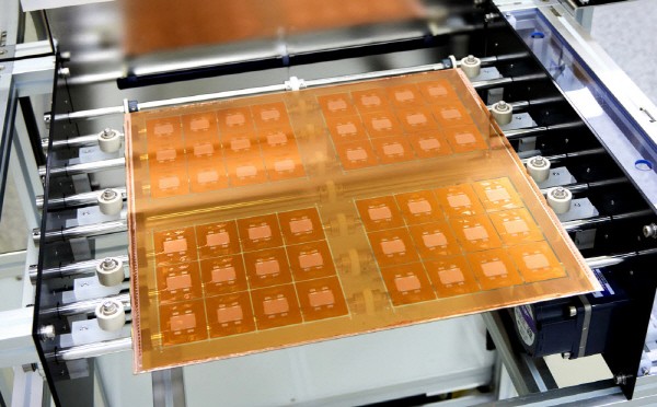
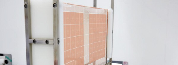
カスタム Glass クラス パッケージ基板について
ガラス基板とは?
ガラス基板 薄いです, 高純度ガラス製の硬質材料, 半導体パッケージングの基礎層として機能するように設計されています. 従来の有機またはシリコンベースの基板とは異なります, ガラスは優れた機械的および電気的特性を提供します, 高度なパッケージング ソリューションに最適な選択肢となる. カスタムガラスクラスパッケージ基板 次世代半導体デバイスの性能と信頼性を向上させるために特別に設計されています. 高密度相互接続のための安定したプラットフォームを提供します, AI のアプリケーションにとって重要, ハイパフォーマンスコンピューティング, および5G通信.
ガラス基板の主な材料特性
の利点 カスタムガラスクラスパッケージ基板 独特の素材特性に由来する:
- 低誘電損失: ガラスは誘電率が大幅に低い (DK) と損失正接 (Df) 有機基板と比較して, 高周波アプリケーションでのより高い信号整合性とクロストークの低減を可能にします.
- 高い熱安定性: 優れた耐熱性を備えています, ガラス基板は極端な温度に耐えることができます, 要求の厳しい電子環境における信頼性の確保.
- 優れた機械的剛性: ガラスは高い剛性と低い反りを示します, これは多層半導体パッケージングの寸法安定性を維持するために重要です.
ガラス基板 vs. 有機基質: 利点と制限事項
有機基板は半導体パッケージングに広く使用されていますが、, カスタムガラスクラスパッケージ基板 いくつかの重要な利点を提供します:
| 特徴 | ガラス基板 | 有機基質 |
|---|---|---|
| 誘電率 | より低い, 高速信号に適しています | より高い, 信号損失の増加につながる |
| 熱安定性 | 素晴らしい, 高温に耐える | 限定, 熱膨張しやすい |
| 機械的強度 | 高剛性, 最小の反り | 剛性の低下, 変形しやすい |
| 小型化 | ファインピッチ化と高密度化が可能 | 超微細ピッチの用途に限定される |
| 製造コスト | より高い, 複雑な処理のため | より低い, 確立された製造プロセス |
半導体パッケージングにおけるカスタムガラスクラスパッケージ基板の役割
半導体デバイスは性能が向上しながらも小型化が続くため、, シグナルインテグリティに対するより高い要求を満たすために、パッケージング技術は進化する必要がある, 電力効率, および熱管理. カスタムガラスクラス パッケージ基板 革命を起こしている 半導体パッケージ 従来の有機基板に代わる先進的な代替品を提供することにより、, 優れた電気特性を提供します, 機械的安定性, および熱性能.
包装用ガラス基板: 信号の整合性と熱管理の強化
カスタム ガラス クラス パッケージ基板の主な利点の 1 つは、信号の整合性を大幅に向上できることです。. 誘電率が低い (DK) 誘電損失が最小限に抑えられています (Df), ガラス基板により、より高速で信頼性の高いデータ伝送が可能になります, AIプロセッサなどの高周波アプリケーションに最適です。, 5Gネットワーク, および高性能コンピューティング (HPC). さらに, ガラスは優れた熱安定性を示します, 反りを軽減し、放熱性を向上させます。. これにより、より優れた熱管理が可能になります, これは、高密度に実装された半導体デバイスの過熱を防ぐために重要です.
TSMCガラス基板イニシアチブ: ガラスを高度なパッケージングに統合
TSMC, 半導体製造のリーダー, チップ性能の限界を押し上げるために、カスタム ガラス クラス パッケージ基板テクノロジーを積極的に研究してきました。. 同社はガラス基板を自社の先進的なパッケージングのロードマップに組み込んでいます, 特にチップレット アーキテクチャと高帯域幅メモリの場合 (HBM) アプリケーション. ガラスの優れた電気絶縁性と機械的安定性を活用することで、, TSMCは消費電力を削減しながら相互接続密度を向上させることを目指しています, 次世代の半導体ソリューションを可能にする.
サムスン & LG Innotek ガラス基板の取り組み: イノベーションと製造能力
Samsung と LG Innotek もカスタムガラスクラスパッケージ基板の開発で大幅な進歩を遂げています. サムスンは、高度な半導体パッケージング用のガラス処理を最適化する大量生産技術に焦点を当てています, 特にAIアクセラレータとモバイルプロセッサにおいて. その間, LG Innotekはガラス基板の製造性を高める革新的な製造方法を開発中, より高い歩留まりとコスト効率の高い生産を保証します. 両社はRに多額の投資を行っている&Dはガラス基板技術を磨き上げる, 有機半導体パッケージングからガラスベースの半導体パッケージングへの移行における主要プレーヤーとしての地位を確立.
ガラス基板 vs. 有機基質: 比較の概要
有機基板は、その低コストと確立された製造プロセスにより、半導体パッケージング業界を支配してきました。, カスタムガラスクラスパッケージ基板は、次世代デバイスに明らかな利点をもたらします:
| 特徴 | ガラス基板 | 有機基質 |
|---|---|---|
| シグナルインテグリティ | 高い, 誘電損失が低いため | 適度, より高い周波数では制限される |
| 熱伝導率 | 素晴らしい, より良い熱放散をサポートします | より低い, 追加の冷却ソリューションが必要な場合 |
| 機械的安定性 | 硬い, 最小の反り | 膨張や変形が起こりやすい |
| 相互接続密度 | 高い, より細かいピッチとスケーリングが可能になります | 材料上の制約による制限 |
| 料金 | より高い, しかし量産により改善 | より低い, 既存のパッケージに広く使用されている |
ガラスコア基板: カスタムガラスクラスのパッケージ基板を使用した次世代のパッケージング
半導体デバイスが前進し続けています, シリコンや有機基板などの従来のパッケージング材料は、物理的および電気的限界に達しつつあります. これらの課題を克服するには, 革新的なソリューションとして登場したカスタムガラスクラスパッケージ基板, 次世代半導体パッケージングをリードするガラスコア基板を使用. ガラスの優れた素材特性を活かして, このテクノロジーはハイパフォーマンス コンピューティングを変革しています, AI, および5Gアプリケーション.
ガラスコア基板とは?
ガラスコア基板は、有機またはシリコンベースの材料の代わりにガラスを中心構造層として使用する一種の先進的な半導体パッケージ材料です。. 従来の基板とは異なります, 有機ラミネートまたはシリコンウェーハに依存するもの, ガラスコア基板は独自の電気絶縁性の組み合わせを提供します, 機械的剛性, および熱安定性. カスタムガラスクラスパッケージ基板 ガラスコアを使用すると、より微細な配線ピッチが可能になります, 信号の整合性が向上しました, 熱性能の向上, チップレット アーキテクチャと高帯域幅メモリにとって理想的な選択肢となります。 (HBM) 統合.
シリコン基板や有機基板に対するガラスコア基板の利点
従来の梱包材との比較, カスタムガラスクラスパッケージ基板 ガラスコアを使用すると、いくつかの重要な利点が得られます:
| 特徴 | ガラスコア基板 | シリコン基板 | 有機基質 |
|---|---|---|---|
| 電気性能 | 低損失, より良い信号の完全性 | 高損失, 消費電力が高い | 適度, ただし高周波では制限される |
| 熱膨張 (CTE) | 半導体材料に適合, ストレスを軽減する | 高い, 潜在的な信頼性の問題につながる | より高い拡張性, 反りの原因となる |
| 機械的剛性 | 高剛性, 低い反り | 脆い, ひび割れしやすい | フレキシブル, ただし変形しやすい |
| 製造コスト | 適度, 量産で改善する | 高い, 複雑な処理のため | 低い, ただしハイエンドアプリケーションには限定されます |
| 小型化 | より微細な相互接続と高密度を実現 | 機械的脆弱性による制限 | 材料特性による制限 |
これらの特性を組み合わせると、 カスタムガラスクラスパッケージ基板 ガラスコアを使用しており、高速データ伝送が必要な用途に最適です。, 小型化, 堅牢な信頼性.
大手半導体企業がガラスコア基板を採用
~の利点を認識する カスタムガラスクラスパッケージ基板, 大手半導体企業はガラスコア基板技術に積極的に投資している:
- TSMC 先進的なパッケージング ソリューションを強化するためにガラス コア基板を開発中, InFOやCoWoSなど, AI および HPC チップの相互接続密度の向上を可能にする.
- インテル ガラス基板研究の大幅な進歩を発表, ガラスコア技術を次世代プロセッサに統合して、電力効率と熱性能を向上させることを目指しています.
- サムスン AIアクセラレータと5Gインフラストラクチャに対する需要の高まりに応えるため、ガラス基板の生産能力を拡大しています.
- LGイノテック 大規模生産に向けて製造技術を改良中, 新興ガラス基板市場における主要サプライヤーとしての地位を確立.
業界リーダーが半導体パッケージングの限界を押し広げ続ける中、, カスタムガラスクラスパッケージ基板 ガラスコアを備えた製品は、次の技術進歩の波で重要な役割を果たすことが期待されています. 製造技術とコスト削減戦略の継続的な改善により、, ガラス基板は、高性能半導体アプリケーションの新たな業界標準となる予定です.
カスタムガラスクラスパッケージ基板の主な利点
半導体技術が進歩するにつれて, パッケージング ソリューションは、より高いパフォーマンスに対する需要の高まりに対応する必要があります, より高い信頼性, 小型化の強化. カスタムガラスクラスパッケージ基板 その独特の材料特性により、従来の有機およびシリコンベースの基板の優れた代替品として浮上しつつあります。. 電気的性能の向上から優れた機械的強度へ, カスタムガラスクラスパッケージ基板 先進的な半導体パッケージングの新たな標準を確立しています.
1. 電気性能: 信号損失の低減, より優れたインピーダンス制御
主な利点の 1 つは、 カスタムガラスクラスパッケージ基板 その優れた電気的特性は. ガラスは誘電率が低い (DK) 誘電損失と (Df) 有機基板と比較して, 信号損失を大幅に削減し、高周波性能を向上させます。. これにより、ガラス基板はAIプロセッサなどのアプリケーションに最適になります。, 5Gネットワーク, および高性能コンピューティング (HPC), 信号の完全性を維持することが重要な場合. さらに, カスタムガラスクラスパッケージ基板 より正確なインピーダンス制御が可能になります, 信号の歪みを最小限に抑え、半導体デバイスの全体的な電力効率を向上させます。.
2. 機械的強度: 有機基板と比較して剛性が高い
機械的安定性は半導体パッケージングにおいて重要な要素です, 反りや変形はデバイスの性能や信頼性に影響を与える可能性があるため. カスタムガラスクラスパッケージ基板 有機基板と比較して剛性が高く、反りが少ない, 製造段階および運用段階での構造的完全性の向上を保証する. 有機基板とは異なります, 高温や機械的ストレス下で変形する可能性があります, ガラス基板はその形状と寸法精度を維持します, チップレット統合や 2.5D/3D スタッキングなどの高度なパッケージング技術により適したものになります。.
3. 熱管理: 放熱特性の向上
熱放散は高性能半導体デバイスにおける大きな課題です. カスタムガラスクラスパッケージ基板 高い熱安定性と効率的な熱伝導特性により、熱管理に優れています。. 有機基板とは異なります, 熱伝導率が低いため、追加の放熱ソリューションが必要になる場合があります, ガラス基板は自然に優れた熱拡散をサポートします, ホットスポットを削減し、システム全体の信頼性を向上させます。. これにより、 カスタムガラスクラスパッケージ基板 高出力アプリケーションに特に有利, データセンターを含む, 自動車エレクトロニクス, AIアクセラレータと.
4. 小型化: より薄くすることが可能, 先進的なデバイス向けのよりコンパクトな設計
半導体パッケージングのトレンドがさらなる小型化に向かう中, カスタムガラスクラスパッケージ基板 超薄型化を可能にする上で重要な役割を果たします, 高密度設計. ガラス基板により、より微細な配線ピッチが可能, より高い配線密度, 平面性も向上, より多くのコンポーネントをより小さな設置面積に統合するために不可欠です. 有機基板との比較, ガラスは優れた表面平坦性を提供します, これにより、高度なリソグラフィープロセスの精度が向上し、よりコンパクトで電力効率の高い半導体デバイスが可能になります。. これは、次世代モバイル プロセッサにとって特に有益です。, ウェアラブル技術, 超小型AIチップ.
ガラス vs. シリコン基板: カスタムガラスクラスパッケージ基板の主な違い
半導体パッケージング技術の進化に伴い, 業界は性能を向上させるために従来のシリコン基板の代替品を模索しています。, コストを削減する, スケーラビリティの向上. カスタムガラスクラスパッケージ基板 有望な解決策として浮上しました, 製造効率の点でシリコン基板に比べて独自の利点を提供します, 電気的および熱的特性, 全体的な費用対効果. このセクションでは、次の主な違いについて説明します。 カスタムガラスクラスパッケージ基板 およびシリコン基板, 先進的な半導体パッケージングにおいてガラスが注目を集めている理由を強調する.
1. 製造プロセスのバリエーション
の製作 カスタムガラスクラスパッケージ基板 シリコン基板とは大きく異なります. シリコンベースの基板は通常、高温酸化を伴うウェハ製造プロセスを使用して製造されます。, ドーピング, フォトリソグラフィ, そしてエッチング. これらのプロセスには高度な半導体グレードのシリコンウェーハが必要です, 製造にはコストがかかり、複雑です.
対照的に, カスタムガラスクラスパッケージ基板 確立されたガラス製造技術を活用, 精密ガラス切断を含む, 化学強化, マイクロビアドリリング, およびメタライゼーション. 大型ガラスパネルを使用したガラス基板の製造が可能, シリコンウェーハよりも高い歩留まりとコスト効率の高い生産が可能になります. さらに, ガラス貫通ビアなどの先進技術 (TGV) 優れた電気的性能を維持しながら、高密度の相互接続が可能になります。.
| 特徴 | カスタムガラスクラスパッケージ基板 | シリコン基板 |
|---|---|---|
| 基材 | 高純度ガラス | 単結晶シリコン |
| 製造工程 | パネルベース, スケーラブルな | ウェーハベース, 複雑な |
| フォーメーション経由 | ガラス貫通ビア (TGV) | シリコン貫通ビア (TSV) |
| スケーラビリティ | 量産用大型パネル | ウェハサイズに制限される |
2. 電気的および熱的特性の比較
カスタムガラスクラスパッケージ基板 電気絶縁性と熱膨張特性の点でシリコンに比べて大きな利点があります. シリコン, 半導体であること, 漏れ電流を防ぐために追加の絶縁層が必要です, 一方、ガラスは本質的に優れた電気絶縁体です. これにより、寄生容量が低減され、高周波アプリケーションにおける信号の完全性が向上します。.
熱膨張も重要な要素です. シリコンは熱膨張係数が高い (CTE) 半導体チップとのミスマッチ, 機械的ストレスや信頼性の問題につながる可能性があります. カスタムガラスクラスパッケージ基板, しかし, 半導体材料に近いCTEを持っています, ストレスを軽減し、高性能アプリケーションにおける長期信頼性を向上させます。.
| 財産 | カスタムガラスクラスパッケージ基板 | シリコン基板 |
|---|---|---|
| 誘電率 | より低い (シグナルインテグリティの向上) | より高い (追加の断熱材が必要) |
| 電気絶縁 | 素晴らしい | 酸化層が必要 |
| 熱膨張 (CTE) | 半導体材料に適合 | チップとの不一致 |
| 放熱 | 適度 | 高い |
3. コストの考慮事項と拡張性
半導体パッケージングにおける最大の課題の 1 つは、コストと拡張性のバランスです。. シリコン基板は優れた性能を発揮しますが、, 半導体グレードのシリコンウェーハと複雑な製造プロセスのコストが高いため、製造コストが高くなります。. 対照的に, カスタムガラスクラスパッケージ基板 材料コストが低く、大型パネル形式で製造できるため、よりコスト効率の高い代替品を提供します。, 生産効率の向上.
スケーラビリティも重要な利点です カスタムガラスクラスパッケージ基板. より大きなパネルサイズでのガラス基板の製造が可能, より高いスループットを実現し、ユニットあたりのコストを削減します. このため、ガラスは先進的な半導体パッケージの大量生産にとって魅力的な選択肢となります。, チップレットを含む, 高帯域幅メモリ (HBM), AIアクセラレータと.
| 要素 | カスタムガラスクラスパッケージ基板 | シリコン基板 |
|---|---|---|
| 材料コスト | より低い (ガラスが豊富にある) | より高い (シリコンウェーハは高価です) |
| 製造コスト | より低い (スケーラブルなパネルベースのプロセス) | より高い (ウェハベースの, 複雑なプロセス) |
| スケーラビリティ | 高い (大きなパネルサイズ) | ウェハサイズに制限される |
業界での採用 & カスタムガラスクラスパッケージ基板の今後の動向
企業が性能を向上させるための新しいパッケージング ソリューションを模索する中、半導体業界は大きな変化を迎えています。, 消費電力を削減する, より高い相互接続密度を実現します. カスタムガラスクラスパッケージ基板 従来のシリコンや有機基板に代わる次世代の基板として注目を集めています, 優れた電気的性能を提供, 機械的安定性, とスケーラビリティ. 高性能コンピューティングの需要として (HPC), 人工知能 (AI), そして5Gテクノロジーは成長する, 大手半導体メーカーと市場アナリストは次のように予測しています。 カスタムガラスクラスパッケージ基板 先進的なパッケージングの将来において重要な役割を果たすことになる.
インテルガラス基板の開発: 彼らのアプローチと市場への影響
インテルはその最前線に立っています カスタムガラスクラスパッケージ基板 研究開発, 現在の包装材料の限界に対処することを目的としています. 同社はガラス基板技術の進歩を公表した, マルチチップパッケージングと高密度相互接続に革命をもたらす可能性を強調.
インテルのアプローチは、 カスタムガラスクラスパッケージ基板 達成する:
- より高い相互接続密度: ガラスにより、より細かい線間隔とより小さなビアサイズが可能になります, 高度なチップレット アーキテクチャにとって重要.
- 優れた熱性能: 改善された熱放散により、AI アクセラレータと高性能プロセッサの増大する電力需要のサポートに役立ちます.
- 消費電力の削減: 誘電損失が低いため、信号の完全性が向上します, 電力漏れを削減し、効率を向上させる.
統合することで カスタムガラスクラスパッケージ基板 パッケージ化ロードマップに組み込まれる, インテルは、より高いトランジスタ密度とより効率的な電力供給ネットワークを可能にすることでムーアの法則を拡張することを目指しています. 同社は、ガラス基板が次世代チップ設計の変革をもたらすと期待している, 特に高性能サーバープロセッサとAIチップにおいて.
Yole グループの洞察: 市場動向と包装大手間の競争
市場調査会社Yole Groupは、 カスタムガラスクラスパッケージ基板, TSMCのような大手企業からの投資増加に注目, サムスン, LGイノテック, およびASEグループ. Yoleの最新レポートによると, 半導体パッケージングにおけるガラス基板の需要は、:
- 高周波アプリケーション: AI, 5g, 高速コンピューティングには、信号損失が低く、インピーダンス制御が優れた基板が必要です.
- 小型化の傾向: ガラス基板により薄型化が可能, よりコンパクトな梱包ソリューション, モバイルおよびウェアラブルデバイスに不可欠な.
- 高度なマルチチップパッケージング: チップレットベースのアーキテクチャの人気が高まるにつれて, ガラス基板はより優れたルーティング機能を提供し、クロストークを低減します.
大手包装大手間の競争が激化, 企業が商品化を競う中、 カスタムガラスクラスパッケージ基板 テクノロジー. Intel と TSMC が R で先頭に立っている一方で、&D, サムスンとLGイノテックは量産能力に多額の投資を行っている, ガラス基板市場における主要サプライヤーとしての地位確立を目指す.
今後の展望: 2.5D および 3D パッケージングの大量採用
の将来 カスタムガラスクラスパッケージ基板 2.5D および 3D パッケージングの進化と密接に関係しています. ガラス基板には、これらの高度なパッケージング技術に最適ないくつかの利点があります。:
- 2.5D 統合: ガラス基板により、シリコンベースの代替品と比較して優れた電気的性能を備えた高密度インターポーザーが可能になります.
- 3D スタッキング: 熱膨張係数が低い (CTE) 積層されたダイ間の応力を軽減します, 信頼性と寿命の向上.
- パネルレベルのパッケージング (PLP): 大型パネルのガラス基板製造が可能となり生産効率が向上, 大量導入に向けたコストの削減.
製造技術の継続的な進歩により、, カスタムガラスクラスパッケージ基板 次世代半導体デバイスの主流ソリューションとなることが期待されています. 大手半導体企業が革新を続ける中、, ガラス基板はハイパフォーマンスコンピューティングにおいて従来の材料に取って代わる可能性が高い, AIプロセッサ, およびネットワークインフラストラクチャ, 半導体パッケージングの未来を形作る.