株式会社")
高度なパッケージ基板メーカー。私たちの会社は、高度なパッケージ基板の製造を専門としています, さまざまな電子アプリケーションに高品質のソリューションを提供します. 私たちは最先端のテクノロジーと革新的な素材を利用して、優れたパフォーマンスを確保する製品を提供します, 信頼性, そして耐久性. 私たちの基質は、現代の電子機器の厳しい要求を満たすように設計されています, 消費者向けガジェットから産業用システムまであらゆるものをサポート. 精度と効率を重視, 当社は最先端の基板ソリューションを通じてエレクトロニクスの未来を前進させることに全力で取り組んでいます。.
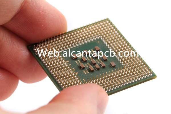
アドバンストパッケージ基板とは?
高度な パッケージ基板 (APS) 現代の電子機器に不可欠なコンポーネントです, 半導体チップやその他のマイクロエレクトロニクス部品の基盤として機能します. 従来のプリント基板とは異なります (プリント基板), APS は、システムインパッケージなどの高度なパッケージング技術の要求を満たすために、より複雑かつ高精度に設計されています。 (SiP) および3D IC. これらの基材は、必要な機械的サポートを提供する役割を果たします。, 電気接続, 集積回路の最適なパフォーマンスを確保するために必要な熱管理 (IC).
APS は通常、複数のレイヤーで構成されます, それぞれが信号送信などの特定のタスクを処理するように設計されています, 配電, そして放熱. これらの基板の複雑さにより、より多くの機能をより小さなフォームファクターに統合することが可能になります。, これはエレクトロニクス業界で進行中の小型化傾向において極めて重要です. 高性能コンピューティングに対する需要の高まりに伴い、, モバイルデバイス, および高度なパッケージングを必要とするその他のアプリケーション, APS は、望ましいレベルのパフォーマンスと信頼性を達成する上で極めて重要な役割を果たします.
構造的および電気的な役割に加えて、, APS は電子機器製造の全体的な費用対効果にも貢献します. スペースと材料のより効率的な利用を可能にする, これらの基板は、最終製品のサイズとコストの削減に役立ちます. さらに, APS を使用すると、製造時の歩留まりが向上します。, 最新の半導体プロセスの厳しい要件に対応するように設計されているため、.
全体, アドバンストパッケージ 基板 電子機器の進化を支える重要な技術です. 複雑なコンポーネントの統合が可能になります。, ますます小型化するパッケージ内の高密度 IC, 家庭用電化製品から電気通信などの分野にイノベーションへの道を切り開く.
アドバンストパッケージ基板デザインリファレンスガイド
先進的なパッケージ基板の設計には、材料科学と電気工学の両方に対する深い理解が必要な細心のプロセスが必要です。. 目標は、電子パッケージの特定のニーズを満たす基板を作成することです。, シグナルインテグリティなどの要素を考慮して, 電力供給, 熱管理, 機械的安定性. 設計プロセスは、基板に実装される IC の要件を定義することから始まります。, レイヤー数も含めて, 信号トレースのルーティング, 電源プレーンとグランドプレーンの配置.
APS 設計における重要な課題の 1 つは、シグナル インテグリティの管理です。. 電子信号の周波数が高くなるにつれて, 信号損失の可能性, クロストーク, 電磁干渉 (EMI) も上がります. これらの問題に対処するには, 設計者は基板のレイアウトを慎重に計画する必要がある, 干渉を最小限に抑えるために、信号トレースが適切な間隔で配置され、シールドされていることを確認します。. 高度なシミュレーション ツールは、さまざまな条件下での基板の動作をモデル化するためによく使用されます。, 設計者が製造段階に移る前にレイアウトを最適化できるようにする.
熱管理は APS 設計のもう 1 つの重要な側面です. 高性能 IC は大量の熱を発生します, コンポーネントへの損傷を防ぎ、信頼性の高い動作を確保するには、この電力を効率的に消散する必要があります。. 設計者はサーマルビアを組み込むことができます, ヒートシンク, 熱の流れを管理するための基板へのその他の冷却機構. 材料の選択も熱性能に重要な役割を果たします, 一部の材料は他の材料よりも熱伝導率が優れています.
電力供給も APS 設計において同様に重要です. 基板は、電圧降下と電力損失を最小限に抑えながら、IC に安定した電力を供給できなければなりません。. これには、電源プレーンとグランドプレーンを慎重に計画する必要があります。, 電圧変動を平滑化するためのデカップリングコンデンサの配置. 電力供給ネットワークの設計 (PDN) 電子パッケージの全体的なパフォーマンスと信頼性を確保する上で重要な要素です.
アドバンストパッケージ基板に使用されている材料?
アドバンストパッケージ基板の材料の選択は、その設計と性能の重要な側面です。. 使用される材料は電気的観点からの厳しい要件を満たさなければなりません, 熱, および機械的特性. 通常, APSは有機材料と無機材料の組み合わせで構成されています, それぞれが特定の属性に応じて選択されます.
APS で使用される最も一般的な材料の 1 つは、一種の高性能樹脂です。, エポキシやポリイミドなど, 基板の誘電体層として機能します. これらの材料は優れた電気絶縁性を発揮します, 半導体製造プロセスに伴う高温に耐えることができます。, 高度な実装に必要なファインピッチ機能にも対応. 断熱特性に加えて、, これらの樹脂は、基板層を一緒に保持するために必要な機械的サポートも提供します。.
基板内の導電性トレースおよびプレーン用, 銅は導電率が高いため、最適な材料です。, 優れた熱伝導性, そして比較的低コスト. 銅線は信号を配線し、基板全体に電力を分配するために使用されます。, 耐久性を高め、信頼性の高いはんだ接続を確保するために、多くの場合、ニッケルと金の薄い層でメッキされています。.
銅や樹脂に加えて, APS にはセラミックフィラーなどの他の材料が組み込まれる場合もあります, 熱伝導率と寸法安定性を向上させるために誘電体層に添加されます。. これらのフィラーは、IC からの熱の放散に役立ちます。, 熱損傷のリスクを軽減し、パッケージの全体的な信頼性を向上させます。.
APS の材料の選択は表面仕上げにも及びます, これは、良好なはんだ付け性を確保し、酸化や湿気などの環境要因から基板を保護するために重要です。. 一般的な表面仕上げには、無電解ニッケル浸漬金が含まれます (同意する), 有機はんだ付け性保存剤 (OSP), 浸漬錫または銀, それぞれがアプリケーションに応じて異なる利点を提供します.
アドバンストパッケージ基板のサイズはどのくらいですか?
アドバンストパッケージ基板のサイズはアプリケーションに応じて大幅に異なる場合があります, 集積回路の複雑さ, 使用されているパッケージング技術. 従来のPCBとは異なり, サイズに関して標準化されることが多い, APS は通常、サポートする電子パッケージの特定のニーズを満たすようにカスタム設計されています。. このカスタマイズにより、幅広いサイズが可能になります, コンパクトなモバイルデバイスで使用される非常に小さな基板から、ハイパフォーマンスコンピューティングアプリケーション向けに設計された大きな基板まで.
システムインパッケージなどの高度なパッケージング技術 (SiP) または3D IC, 基板のサイズは、多くの場合、収容する必要がある IC の設置面積によって決まります。. 例えば, SiP内で, 複数のICと受動部品が単一のパッケージに統合されています, 基板は、信号と電力の効率的な配線を可能にしながら、これらすべてのコンポーネントを収容するのに十分な大きさでなければなりません。. 場合によっては, 基板は各辺が数ミリメートルほど小さい場合があります, 特にスペースが貴重なアプリケーションでは, ウェアラブルデバイスや埋め込み型医療機器など.
一方で, より複雑な機能や高いパフォーマンスを必要とするアプリケーション向け, より大きな基板を使用することもできる. これらの基板は各辺が数センチメートルになることがあり、必要な相互接続と電源プレーンの数の増加をサポートするために複数の層が含まれる場合があります。. ハイパフォーマンスコンピューティングでは, 例えば, 基板は、IC だけでなく、広範な電源および接地ネットワークにも対応する必要があります, 熱管理機能, そして場合によっては埋め込まれた受動部品も.
APS の厚さは、用途に応じて変化するもう 1 つの重要な寸法です。. 機械的強度が懸念される用途では、通常、より厚い基板が使用されます。, 一方、スペースの節約が重要な用途では、より薄い基板が好まれます。. 基板の厚さも熱性能に影響します, より厚い基板を使用すると、通常、より優れた放熱機能が得られます.
アドバンストパッケージ基板の製造プロセス
アドバンストパッケージ基板の製造プロセスは、精度と厳格な品質基準の順守が必要な、非常に洗練された複数のステップからなる手順です。. プロセスはベース材料の準備から始まります, 通常、導電性材料と絶縁性材料の両方を組み合わせた多層構造の製造が含まれます。. 最初のステップでは、誘電体層の積層が行われます。, 通常は高性能樹脂で作られています, 銅箔付き. これらの層は一連のフォトリソグラフィー工程を通じて処理され、回路パターンが定義されます。.
フォトリソグラフィーは、フォトレジスト材料と紫外線を使用して、所望の回路パターンを銅層に転写する重要なプロセスです。 (紫外線) ライト. 次に、露光された領域が現像されます, 露光されていない領域はエッチングで除去されます, 基板内に電気経路を形成する銅のトレースを残す. このプロセスを複数回繰り返して、必要な数の層を構築します。, 各層は慎重に位置合わせされ、基板全体で適切な電気的接続が確保されます。.
フォトリソグラフィーとエッチングのプロセスを経て、, 基板はその表面特性を改善するために一連の化学処理を受けます, 密着性やはんだ付け性など. 無電解ニッケル浸漬金のような表面仕上げ (同意する) または有機はんだ付け性保存剤 (OSP) 銅トレースを保護し、後続のはんだ付けプロセスに備えるために適用されます。. これらの仕上げは、基板とその上に実装される IC 間の信頼性の高い接続を確保するために非常に重要です。.
穴あけは製造プロセスのもう 1 つの重要なステップです, 基板の異なる層間の電気接続を確立するためにマイクロビアとスルーホールが作成される場所. これらのビアは、導電性を確保するために銅でメッキされます。. 高度な穴あけ技術, レーザー穴あけなど, 高密度基板に必要な精密かつ小径のビアを実現するためによく使用されます。.
ついに, 完成した基板は厳格なテストと検査を受け、要求仕様を満たしていることを確認します。. これには、接続を確認するための電気テストが含まれます, 熱放散能力を評価するための熱試験, 基材の強度と耐久性を評価するための機械的試験. これらのテスト中に検出された欠陥は、再作業または再作業によって対処されます。, 場合によっては, 電子機器製造に必要な高い基準を維持するために基板は廃棄されます.
アドバンストパッケージ基板の応用分野
先進的なパッケージ基板は、幅広い業界やアプリケーションで利用されています, 現代のエレクトロニクスにおけるその多用途性と重要な役割を反映しています. これらの基板は、高性能を実現するための基礎となります。, 小型化, 今日の高度な電子システムに求められる信頼性. 主な応用分野の 1 つは半導体産業です。, 特にシステムインパッケージなどの高度なパッケージング技術において (SiP), 3D IC, およびフリップチップボールグリッドアレイ (FC-BGA).
家庭用電化製品の分野では, APS はスマートフォンの機能に不可欠です, 錠剤, ウェアラブルデバイス, およびその他のポータブルガジェット. これらのデバイスには、小さな設置面積を維持しながら高密度の相互接続をサポートできる基板が必要です。. APS のコンパクトなサイズと複雑さにより、単一のパッケージ内に複数の機能を統合できます。, デバイス全体のサイズと重量を削減しながら、パフォーマンスとバッテリー寿命を向上させます。.
自動車産業も APS の重要な応用分野です, 特に車両がエンジン制御ユニットに至るまでの機能を電子システムに依存するようになったため、 (ECU) 先進運転支援システムまで (ADAS) そしてインフォテイメント. 自動車用途の APS は、厳しい信頼性と耐久性の基準を満たさなければなりません, 過酷な環境条件にさらされることが多いため、, 極端な温度や振動を含む.
通信で, APS は 5G インフラストラクチャやその他の高周波通信システムの開発において重要です. これらのアプリケーションで使用される基板は、高速データ伝送と処理の要求に対処するために、優れた信号整合性と熱管理を提供する必要があります。. APS により、5G ネットワークやその他の次世代通信技術の展開に不可欠なコンパクトで効率的なモジュールの作成が可能になります.
医療機器も APS の使用から恩恵を受けます, 特に小型化と精度が要求される用途では, 埋め込み型デバイスなど, 診断装置, ウェアラブルヘルスモニターなど. 生体適合性, 信頼性, APS は、複数の機能を単一のパッケージに統合できるため、これらの機密性が高く、多くの場合生命に関わるアプリケーションにとって理想的な選択肢となります。.
アドバンストパッケージ基板の利点は何ですか?
アドバンストパッケージ基板には、高性能電子デバイスの製造に欠かせないいくつかの利点があります。. 最も重要な利点の 1 つは、高密度の相互接続をサポートできることです。, 電子機器の機能が向上する一方でサイズは縮小し続けるため、これは非常に重要です。. より多くのコンポーネントと接続をより小さなスペースに詰め込むことができるため、よりコンパクトな製品を作成できます。, 強力な, エネルギー効率の高いデバイス.
APS のもう 1 つの重要な利点は、優れた熱管理機能です。. ICの高性能化に伴い, より多くの熱を生成します, 信頼性の高い動作を確保するには、これを効率的に消散する必要があります. APS は高度な熱管理機能を備えて設計されています, サーマルビアなど, ヒートシンク, 熱伝導率の高い素材を使用, 取り付けられたコンポーネントから発生する熱を効果的に管理するため. これにより、電子パッケージの全体的な信頼性と寿命が向上します。.
APS は優れた電気的性能も提供します, 特に信号の完全性と電力供給の観点から. これらの基板の正確な設計と構造により、信号損失を最小限に抑えることができます。, クロストーク, 電磁干渉 (EMI), 高周波信号のパフォーマンスを維持するために重要です. さらに, 最適化された電力供給ネットワーク (PDN) APS 内で IC が安定したクリーンな電力を確実に受け取ることができるようにする, 電源関連の障害のリスクを軽減する.
APS の多用途性も大きな利点です. 幅広いアプリケーションの特定のニーズを満たすようにカスタム設計できます。, 家庭用電化製品から自動車システム、医療機器まで. この柔軟性により、メーカーは製品の正確な要件に合わせて基板を調整することができます。, パフォーマンスとコスト効率の向上につながります.
ついに, APS は電子機器製造の全体的な費用対効果に貢献します. 複数の機能を単一のパッケージに統合できるようにすることで、, 追加のコンポーネントや相互接続の必要性が軽減されます。, 全体的な部品表を削減できる (BOM) そして組み立て費用. さらに, APS 製造プロセスに関連する歩留まりの向上により、欠陥のあるユニットの数が減り、さらなるコスト削減につながる可能性があります。.
よくある質問
アドバンストパッケージ基板と従来の PCB の違い?
アドバンストパッケージ基板は、複雑さの点で従来の PCB とは異なります。, 材料, デザインの焦点. APS は、高密度の相互接続をサポートするように特別に設計されています, SiPや3D ICなどの高度なパッケージング技術, 優れた熱的および電気的性能を提供します. また、IC とそれらが提供するアプリケーションの特定のニーズを満たすようにカスタマイズされています。, PCBとは異なります, より一般化されたもの.
アドバンストパッケージ基板の標準的な寿命はどれくらいですか?
APS の寿命は、アプリケーションと動作条件によって異なります。. しかし, 通常、長期的な信頼性を考慮して設計されています。, 多くの場合、電子機器自体の寿命と同じくらい長持ちします, 数年から10年以上にわたることもあります.
APSの製造プロセスはPCBの製造プロセスとどのように異なりますか?
APSの製造プロセスにはより高度な技術が必要です, より微細なフォトリソグラフィーなど, マイクロビア用のレーザー穴あけ加工, より複雑な多層構造. APS の製造では、熱管理にも重点が置かれています, シグナルインテグリティ, 従来の PCB 製造と比較した電力供給.
Advanced Package Substrate の使用に制限はありますか??
APS には多くの利点がありますが、, 従来の PCB と比較して、設計と製造にコストがかかる可能性があります. 設計が複雑なため、専門的な知識とツールも必要です, 開発時間とコストが増加する可能性がある. さらに, APS のカスタマイズは、すべてのアプリケーションに適しているわけではないことを意味します, 特に高密度または高性能のパッケージングを必要としないもの.