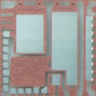
Leadframe&metal frame for QFN Manufacturer, the lead frame material is C-194F.H, Silver plating on the Leadframe(metal frame) or Au plating on Leadframe(metal frame), we produce the QFN metal frame/Leadframe with high quality and fast lead time.
The leadframe is an essential component in the packaging of integrated circuits (ICs), particularly in Quad Flat No-lead (QFN) packages. As modern electronics demand smaller, more efficient, and cost-effective packaging solutions, QFN packages have become highly popular due to their compact size, excellent thermal performance, and electrical reliability. The leadframe, used in QFN packages, plays a critical role in connecting the semiconductor die to external circuits while providing mechanical support and heat dissipation. This article explores the design, function, and benefits of leadframes in QFN packages, along with an overview of the manufacturing process.
What is a Leadframe?
A leadframe is a metallic structure, typically made of copper or copper alloys, designed to support and electrically connect the semiconductor die to external components. In the case of QFN packages, the leadframe forms the foundation that supports the IC die and provides pathways for electrical signals. The unique design of QFN packaging eliminates protruding leads, with electrical connections positioned underneath the package. This flat, leadless configuration results in a smaller form factor compared to traditional packages, making it ideal for space-constrained applications.

Role of the Leadframe in QFN Packages
The leadframe in QFN packages performs two vital functions: electrical connectivity and mechanical support.
1. Electrical Connectivity
In a QFN package, the leadframe provides the connection between the IC die and external circuits. After the die is mounted on the leadframe, wire bonding or flip-chip techniques are used to connect the die’s electrical pads to the leads of the leadframe. These leads, typically located at the edges and bottom of the package, connect to a Printed Circuit Board (PCB) when the package is mounted. The short, flat leadframe design in QFN minimizes inductance and resistance, making it highly suitable for high-speed and high-frequency applications.
2. Mechanical Support and Thermal Management
The leadframe provides mechanical stability during the assembly process and helps to protect the IC during operation. Additionally, the exposed pad on the bottom of the QFN package, which is part of the leadframe, facilitates efficient heat dissipation. This is particularly important in applications where thermal management is critical, as it allows heat to be directly transferred from the die to the PCB, preventing overheating and ensuring stable operation.
Advantages of Using Leadframes in QFN Packages
Leadframes offer several advantages in QFN packages, contributing to their widespread use in various industries:
- Compact Size: QFN packages are small, lightweight, and low-profile, making them ideal for applications where space is limited, such as smartphones, wearable devices, and IoT applications.
- Excellent Thermal Performance: The exposed pad of the leadframe in QFN packages provides a direct thermal path from the IC to the PCB, improving heat dissipation and making the package suitable for high-power applications.
- Cost-Effectiveness: Leadframe manufacturing is a well-established and cost-efficient process. The simplicity of QFN design reduces material usage and production costs, making it an affordable option for high-volume production.
- Superior Electrical Performance: Leadframes in QFN packages provide low-resistance, low-inductance electrical connections. This results in enhanced signal integrity, making QFN packages ideal for applications requiring high-speed data transfer and minimal signal loss.
Manufacturing Process of Leadframes for QFN Packages
The production of leadframes typically involves either stamping or etching a thin sheet of copper or copper alloy into the desired shape. The metal is then plated with materials like silver, gold, or palladium to enhance conductivity and prevent corrosion. After the semiconductor die is mounted on the leadframe, wire bonding or flip-chip bonding is performed to connect the die’s pads to the leads. Encapsulation follows, where a mold compound is applied to protect the IC and leadframe assembly. The final steps include trimming and forming the leads to ensure precise connections with the PCB.
Conclusion
Leadframes are integral to the success of QFN packages, offering reliable electrical connections, mechanical support, and superior thermal performance in a compact form. As electronics continue to shrink in size and increase in complexity, leadframe-based QFN packaging will remain a popular and cost-effective solution for high-performance applications. With their ability to meet the demands of modern electronic devices, leadframes are an indispensable part of the semiconductor packaging industry.
 ALCANTA TECHNOLOGY(SHENZHEN)CO.,LTD