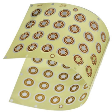
The Thinnest PCB Manufacturer.The Thinnest PCB Manufacturer specializes in producing ultra-thin printed circuit boards that push the boundaries of modern electronics. Their state-of-the-art manufacturing processes and cutting-edge technology enable the creation of incredibly thin PCBs, providing unparalleled performance and flexibility for a wide range of applications, from smartphones to medical devices.
The thinnest PCBs (Printed Circuit Boards) represent a significant advancement in electronic design, enabling ultra-slim and lightweight devices without compromising functionality. These PCBs are essential in applications where space and weight are critical factors. This article delves into the properties, structure, materials, manufacturing processes, applications, advantages, and frequently asked questions (FAQs) related to the thinnest PCBs.
Structure of The Thinnest PCBs
The structure of the thinnest PCBs is meticulously engineered to maintain performance while reducing thickness:
Typically made from high-performance, flexible materials such as polyimide or ultra-thin FR-4 to provide mechanical stability and flexibility.
Extremely thin layers of copper, sometimes as thin as 9 micrometers (μm), are used for conductive traces.
Ultra-thin dielectric materials between conductive layers to ensure electrical insulation without adding bulk.
Specialized adhesives that are thin but strong to bond the layers securely.
Ensures solderability and protects exposed copper from oxidation.

Materials Used in The Thinnest PCBs
Key materials used in the thinnest PCBs include:
A flexible and heat-resistant material ideal for thin PCBs due to its durability and high-performance characteristics.
A thin version of the standard FR-4 laminate used in conventional PCBs, offering good mechanical strength and electrical insulation.
Thin copper foils are used for creating conductive pathways while maintaining minimal thickness.
Materials such as liquid crystal polymer (LCP) or Teflon (PTFE) are used for their excellent electrical properties and minimal thickness.
Thin, high-performance adhesives that maintain integrity and strength without adding significant bulk.
Manufacturing Process of The Thinnest PCBs
The manufacturing process for the thinnest PCBs involves several precise steps to ensure quality and reliability:
Selection and preparation of ultra-thin base materials, copper foils, and dielectrics.
Layers are laminated together under high pressure and temperature using specialized thin adhesives.
Photolithography is used to pattern the copper layers, defining the circuit paths.
Chemical etching removes excess copper, leaving behind the desired circuit patterns.
Precision drilling creates vias and holes for inter-layer connections and component mounting.
Electroplating adds copper to vias, enhancing electrical connectivity.
Application of surface finishes such as ENIG (Electroless Nickel Immersion Gold) to protect the copper and ensure solderability.
Rigorous inspection and electrical testing to ensure the PCB meets design specifications and performance standards.
Applications of The Thinnest PCBs
The thinnest PCBs are used in a variety of high-tech applications:
Smartphones, tablets, and wearable devices where space is at a premium.
Implantable devices and portable medical equipment that require minimal size and weight.
Compact, lightweight electronics for satellites, drones, and military equipment.
Advanced driver-assistance systems (ADAS) and infotainment systems in vehicles.
High-frequency devices and compact communication modules.
Advantages of The Thinnest PCBs
The thinnest PCBs offer several significant advantages:
Allows for the design of ultra-compact and lightweight electronic devices.
Especially when made from materials like polyimide, they can be bent and folded without damage, useful in flexible electronics.
Despite their thinness, they maintain excellent electrical performance and signal integrity.
Efficient heat dissipation despite the compact form factor.
Suitable for a wide range of applications across various industries.
FAQ
What are the main challenges in manufacturing the thinnest PCBs?
Manufacturing the thinnest PCBs involves challenges such as handling ultra-thin materials without damage, maintaining precise alignment during lamination, and ensuring reliable electrical connections with minimal material thickness.
How do the thinnest PCBs compare to traditional PCBs in terms of performance?
The thinnest PCBs can match or even exceed the performance of traditional PCBs in many aspects, including electrical performance and thermal management, thanks to advanced materials and precise manufacturing processes.
What industries benefit the most from the use of the thinnest PCBs?
Industries such as consumer electronics, medical devices, aerospace, automotive, and telecommunications benefit significantly from the use of the thinnest PCBs due to their space-saving and high-performance characteristics.
How do the thinnest PCBs ensure reliability despite their minimal thickness?
The thinnest PCBs ensure reliability through the use of high-quality materials, precise manufacturing processes, and rigorous testing to meet stringent performance and durability standards.
 ALCANTA TECHNOLOGY(SHENZHEN)CO.,LTD