株式会社")
超多層膜 FC-BGA基板 メーカー。最先端の超多層FC-BGA基板メーカーとして, 当社は、最先端の電子アプリケーション向けの高密度相互接続ソリューションの製造を専門としています。. 当社の基板は優れたパフォーマンスを提供します, 熱管理, シグナルインテグリティ, ハイパフォーマンスコンピューティングに最適です, 電気通信, およびデータセンター. 最先端の製造プロセスと厳格な品質管理により、, 当社の製品が最高の業界基準を満たしていることを保証します, お客様に信頼性と革新性を提供する.
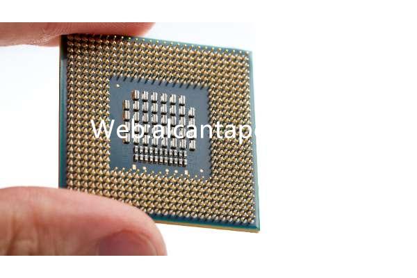
超多層FC-BGA (フリップチップボールグリッドアレイ) 基板 集積回路の接続性とパフォーマンスを向上させるために半導体パッケージングに使用される洗練された回路基板です (IC) およびマイクロプロセッサ. これらの基板は、高密度の相互接続と効率的な熱放散のための堅牢なプラットフォームを提供することにより、現代のエレクトロニクスにおいて重要な役割を果たします。. この記事では、超多層 FC-BGA 基板について詳しく説明します。, 構成の詳細を説明する, 製造工程, アプリケーション, と利点.
超多層FC-BGA基板とは?
超多層 FC-BGA 基板は、複数の導電性材料と絶縁性材料を使用して設計された高度な回路基板です。, フリップチップ技術を使用して半導体デバイスの高密度相互接続を可能にする. これらの基板は通常、ボール グリッド アレイを備えています。 (BGA) 構成, 基板の下側のはんだボールによりプリント基板への電気接続が容易になります。 (プリント基板) または別の基板. 超多層 FC-BGA 基板は層数が多いことが特徴です, ファインピッチ相互接続, 高度な熱管理機能.
超多層FC-BGA基板の構造
超多層 FC-BGA 基板の構造は、電気的性能を最大化するように設計されています。, 熱放散, 機械的安定性. 主要な構造要素には次のものがあります。:
通常はエポキシベースのラミネートなどの高性能材料で作られています (例えば。, FR-4), ポリイミド, または先進的なセラミックス (例えば。, アルミナまたは窒化アルミニウム). 基板材料の選択は、電気特性に関する特定のアプリケーション要件に依存します。, 熱伝導率, そして機械的強度.
導電性トレースの複数の交互層で構成されています (銅または他の金属) および誘電体材料 (樹脂またはガラス強化エポキシ). 多層スタックアップにより、電気信号と電力分配の複雑な配線が可能になります, 高速データ転送をサポートし、信号損失を最小限に抑えます。.
半導体デバイス (IC またはマイクロプロセッサ) フリップチップ技術を使用して基板に直接実装されます, はんだバンプがチップのボンディングパッドを基板上の対応するパッドに接続する場所. この構成により、寄生容量とインダクタンスが低減されます。, 電気的性能の向上.
小さな穴 (ビア) 基板層に穴を開け、導電性材料を充填したマイクロビア (例えば。, 銅) 基板の異なる層間に垂直方向の電気接続を確立するため. マイクロビアは、ファインピッチの高密度相互接続を実現し、信号伝播遅延を低減するために重要です。.
基材の表面に保護層を塗布する, はんだ接続部を除く. はんだマスクにより、はんだ接合の信頼性が向上します, はんだブリッジを防止します, 環境要因から保護します.
基板の下側には、はんだボールが格子状に配置されています。 (BGA構成). これらのはんだボールは、基板を PCB または別の基板に取り付けるための電気接点として機能します。, 信頼性の高い電気的および機械的接続を確保する.
超多層FC-BGA基板に使用される材料
超多層 FC-BGA 基板は、電気的特性を考慮して選ばれた先進的な材料を利用しています。, 熱, および機械的特性, 高速および高周波数アプリケーションの性能要件を満たすように調整されています. 主な材料には以下が含まれます::
オプションにはエポキシベースのラミネートが含まれます (例えば。, FR-4), ポリイミド (例えば。, 船長), または先進的なセラミックス (例えば。, アルミナまたは窒化アルミニウム). これらの材料は、電気絶縁のさまざまな組み合わせを提供します。, 熱伝導率, 多様な用途ニーズに対応する機械的強度と強度.
銅は、高周波回路における優れた導電性と信頼性により、導電性トレースと電源プレーンに使用される主な材料です。. 金や他の貴金属の薄層は、優れた耐食性や電気接触の信頼性が必要な特定の用途に使用できます。.
樹脂系材料 (例えば。, エポキシまたはポリイミド) または、ガラス強化エポキシ積層板が誘電体層として使用され、導電性トレースと層の間に電気絶縁が提供されます。. これらの材料は、高速信号伝送のための低誘電率と制御されたインピーダンス特性を提供します。.
鉛フリーはんだ合金 (例えば。, SAC305) はんだボールや相互接続によく使用されます, 環境規制に準拠し、堅牢な機械的および電気的接続を確保します。.
オプションには有機はんだ付け性保存剤が含まれます (OSP), 浸漬缶 (イムスン), または無電解ニッケル浸漬金 (同意する), はんだ接合の信頼性を高めるために基板の表面に塗布されます, 酸化を防ぎます, 電気接触性能を向上させます.
超多層FC-BGA基板の製造プロセス
超多層 FC-BGA 基板の製造プロセスには、高密度の相互接続を実現するための高度な技術と精密エンジニアリングが必要です。, 最適な電気的性能, と信頼性. このプロセスには通常、次の手順が含まれます:
エンジニアはコンピューター支援設計を使用して基板レイアウトを設計します (CAD) ソフトウェア, 半導体デバイスの配置を指定する, 導電性トレース, ビア, はんだボール.
ベース基板の材質 (例えば。, エポキシベースのラミネートまたはセラミック) 準備され、適切なサイズのパネルに切断されます. 表面処理技術, 洗浄や面粗しなど, 後続の層の接着を促進するために使用されます.
導電性銅箔と誘電体プリプレグの交互層 (樹脂含浸ガラスクロス) またはコア材料を積み重ねて多層スタックアップを形成します. 次に、積層プレスでスタックを圧縮および加熱し、層を結合します。, 固体複合基板の形成.
精密穴あけ装置を使用して、多層スタックにビアやマイクロビア用の穴を作成します。. レーザー穴あけまたは機械穴あけ技術が使用されます, ビアのサイズと密度の要件に応じて.
ビアとマイクロビアは導電性材料でメッキされています (通常は銅) 基板の異なる層間に電気接続を確立するため. 銅メッキの後に貴金属の薄い層を蒸着します。 (例えば。, 金) はんだ付け性を高め、酸化を防ぐために露出した表面に塗布されます。.
基板の外層の導電性銅箔は、化学プロセスまたはフォトリソグラフィーを使用してエッチングされ、回路トレースが定義されます。, パッド, 設計仕様に従った信号経路.
導電性金属の薄層 (例えば。, ゴールドまたはニッケル) はんだ付け可能な表面を作成し、信頼性の高い電気的接触を確保するために、スパッタリングや電気めっきなどの技術を使用して基板の表面に堆積されます。. 表面仕上げ材 (例えば。, OSP, 同意する) 露出した金属表面を保護し、はんだ接合の品質を向上させるために適用されます。.
はんだボールは、自動ディスペンスおよびリフローはんだ付けプロセスを使用して正確に配置され、基板の下面に取り付けられます。. はんだボールはボールグリッドアレイを形成します (BGA) 構成, 基板を PCB または別の基板に取り付けるための電気接点を提供する.
組み立てられた超多層 FC-BGA 基板は、電気的導通を検証するために厳格なテストおよび検査プロセスを受けます。, インピーダンス制御, はんだ接合部の完全性, そして全体的な機能性. テストには電気テストが含まれます, 熱サイクル, X線検査, 自動光学検査 (あおい) 欠陥を検出し、品質を保証するため.
超多層FC-BGA基板の応用分野
超多層 FC-BGA 基板は、高密度の相互接続を必要とする高度な電子アプリケーションで幅広く使用されています。, 優れた電気性能, 信頼性の高い熱管理. 主な応用分野は次のとおりです。:
サーバーで使用される, スーパーコンピューター, 高速データ処理をサポートするデータセンター, 人工知能 (AI), および機械学習アプリケーション.
ネットワークルーターに導入, スイッチ, 高周波信号とデータ伝送を低遅延かつ最小限の信号損失で処理する通信機器.
スマートフォンに統合, 錠剤, 複雑な機能をサポートするウェアラブル デバイス, 高解像度ディスプレイ, 効率的な電源管理.
先進運転支援システムに活用 (ADAS), インフォテイメント システム, 過酷な自動車環境でも信頼性の高い動作を保証する車両制御ユニット.
ロボット工学への応用, オートメーションコントローラー, および産業用IoT (モノのインターネット) リアルタイム制御を可能にするデバイス, 監視, 製造および産業環境におけるデータ処理.
医療用画像機器に使用される, 診断装置, 正確な制御を実現する埋め込み型電子機器, 高い信頼性, ヘルスケア用途における長期的なパフォーマンス.
超多層FC-BGA基板のメリット
超多層 FC-BGA 基板には、高性能電子パッケージングに欠かせないいくつかの利点があります。:
多層スタックアップとファインピッチマイクロビアにより、信号と電力分配の高密度配線が可能になります。, 複雑な電子設計と小型化をサポート.
フリップチップ相互接続と高度な配線技術によって実現された低寄生容量と低寄生インダクタンスにより、高速信号伝送が保証されます。, 信号遅延の減少, 電磁干渉を最小限に抑えます (EMI).
高度なサーマルビア, ヒートシンク, 熱放散技術を効果的に活用
高出力半導体デバイスから発生する熱を放散する, 最適な動作温度を維持し、コンポーネントの寿命を延ばします。.
堅牢な構造, 信頼性の高いはんだ接合, および厳格なテスト手順により長期的な信頼性が保証されます, 機械的安定性, 温度変動や振動などの環境要因に対する耐性.
多様な基板材料への対応, 表面仕上げ, およびアセンブリ技術により、特定のアプリケーション要件に応じたカスタマイズが可能になります, イノベーションと製品の差別化を促進する.
よくある質問
超多層FC-BGA基板はどのようにして高速信号伝送を促進するのか?
高度な配線技術により高速信号伝送を実現する超多層FC-BGA基板, ファインピッチマイクロビア, および低誘電材料, 信号伝播遅延を最小限に抑える, インピーダンスの不整合, 電磁干渉 (EMI).
超多層 FC-BGA 基板でフリップチップ技術を使用する主な利点は何ですか?**
フリップチップ技術によりワイヤボンディングが不要, 電気的性能を向上させながら寄生容量とインダクタンスを低減. また、半導体デバイスと基板間の直接的な熱的および電気的接続も可能になります。, 熱放散と信号整合性の向上.
超多層 FC-BGA 基板が最も一般的に使用されている業界は次のとおりです。?
超多層 FC-BGA 基板は、ハイパフォーマンス コンピューティングなどの業界で主に使用されています。, 電気通信, 家電, 自動車エレクトロニクス, 産業用自動化, および医療機器. これらの業界では、複雑な機能をサポートできる高度なパッケージング ソリューションが求められています。, 高い信頼性, そして効率的なパフォーマンス.
信頼性と品質を確保するための超多層 FC-BGA 基板はどのように製造されているのか?
超多層 FC-BGA 基板は、基板製造を含む綿密な製造プロセスを経ます。, レイヤースタッキング, 掘削, 金属化, 表面仕上げ, はんだボールアタッチメント, そして厳密なテスト. 正確な寸法精度を達成するために、各ステップは慎重に制御されます, 最適な電気的性能, 堅牢な機械的完全性, 高性能電子アプリケーションの厳しい要件を満たします.