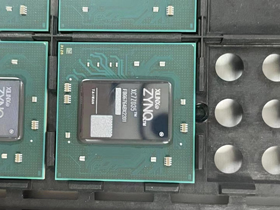
What is the FC BGA Package?
FC BGA, an abbreviation for Flip Chip Ball Grid Array, represents an innovative semiconductor packaging technique that has brought about a revolution in the realm of electronics. It offers an efficient means of connecting the silicon die to the substrate, thereby elevating the performance and reliability of electronic devices to new heights.
At its core, FC BGA involves “flipping” the semiconductor die, so the active side faces down, and connecting it to the package substrate using solder balls. This design minimizes the distance between the die and the package, reducing electrical impedance and improving signal integrity. FC BGA packages are characterized by their grid array of solder balls on the bottom, making them ideal for surface-mount applications.
A standout feature of FC BGA is its exceptional heat dissipation capability, rendering it exceptionally well-suited for high-power devices. Furthermore, the compact form factor of FC BGA packages facilitates the downsizing of electronic devices, a critical factor in the context of contemporary consumer electronics.
FC BGA Package Reference Guide.
In the world of electronic components and semiconductor packaging, FC BGA, or Flip Chip Ball Grid Array, has gained significant prominence.”Comprehending FC BGA packaging is indispensable, whether you’re an electronics enthusiast or a seasoned professional in the industry, due to its array of advantages encompassing enhanced performance, heightened reliability, and streamlined dimensions.”This article serves as a comprehensive reference guide that delves into the intricacies of FC BGA packaging, from its basic definition to cost considerations.
Understanding FC BGA packaging involves delving into its various aspects and considerations. Here’s a reference guide to help you navigate the world of FC BGA packages:
2.1. Design Considerations: FC BGA packages come in various sizes and configurations. Designers must consider factors such as the number of solder balls, pitch, and package size to meet the specific requirements of their electronic devices.
2.2. Materials: The choice of materials for FC BGA packaging plays a crucial role in its performance. Materials should offer high thermal conductivity, low coefficient of thermal expansion, and compatibility with lead-free soldering processes.
2.3. Reliability: FC BGA packages are known for their robustness and reliability. They exhibit excellent resistance to mechanical stress, thermal cycling, and temperature extremes, making them suitable for a wide range of applications.
2.4. Manufacturing Process: FC BGA packaging involves intricate manufacturing processes, including die attach, wire bonding, and solder ball attachment. Understanding these processes is essential for producing high-quality FC BGA packages.
2.5. Applications: FC BGA packaging finds applications in a variety of industries, including consumer electronics, automotive, aerospace, and telecommunications. Its versatility and reliability make it a preferred choice for many critical electronic components.

How Much Does FC BGA Packaging Cost?
The cost of FC BGA packaging varies depending on several factors, including package size, material selection, and production volume. Generally, FC BGA packages are considered a premium packaging option due to their advanced technology and performance benefits.
Cost factors to consider:
3.1. Package Size: Larger FC BGA packages with more solder balls tend to be more expensive than smaller ones. The complexity of the package design also influences the cost.
3.2. Materials: High-quality materials, such as advanced ceramics and high-performance substrates, can increase the cost of FC BGA packaging. However, these materials offer superior thermal and electrical properties.
3.3. Production Volume: The cost per unit decreases with higher production volumes. Manufacturers may offer volume discounts, making FC BGA packaging more cost-effective for large-scale production.
3.4. Additional Features: Specialized features like heat spreaders or advanced thermal solutions can add to the cost of FC BGA packaging but may be necessary for specific applications.
Conclusion: In summary, FC BGA packaging is a sophisticated semiconductor packaging technology that offers numerous advantages in terms of performance, reliability, and size. This comprehensive reference guide has explored the basics of FC BGA packaging, important considerations, and cost factors. Whether you’re designing electronic devices or simply interested in understanding advanced packaging technologies, FC BGA packaging is a topic worth exploring in-depth. Its versatility and reliability continue to drive its adoption in various industries, shaping the future of electronics.
If you have any problem with production process capacity or material, please contact our engineers directly. We will help you sincerely and quickly without any consulting fees. Our email: INFO@ALCANTAPCB.COM
Thank you.
 ALCANTA TECHNOLOGY(SHENZHEN)CO.,LTD