株式会社")
14 レイヤーBGA/IC基板メーカー。主要な14層BGA/IC基板メーカーとして, 高度な半導体パッケージに不可欠な高性能基板の生産を専門としています. 当社の基板は、複合体をサポートするために精度で設計されています, 多層回路基板, 優れた信号の完全性と信頼性を確保します. 最先端のテクノロジーを利用します, 当社は、高速エレクトロニクスおよび高密度アプリケーションの厳しい要件を満たすようにカスタマイズされたソリューションを提供します. 品質と革新に対する当社の取り組みにより、当社は業界の信頼できるパートナーとなっています。, 次世代電子デバイスを駆動する堅牢で効率的な基板を提供.
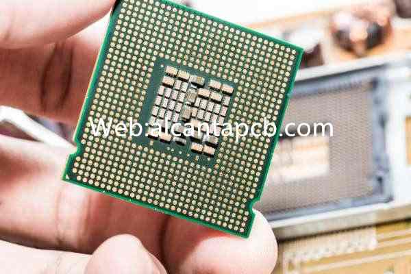
14 レイヤ BGA/IC 基板はエレクトロニクス業界の重要なコンポーネントです, 特に堅牢なパッケージングソリューションを必要とする高性能アプリケーション向け. これらの基板はボール グリッド アレイをサポートしています (BGA) および集積回路 (IC) 梱包, シリコンダイとプリント基板の間に必要な相互接続を提供する (プリント基板). 14 層設計により、配線密度が向上し、電気的性能が向上します。, 複雑な電子機器に最適です. この記事ではその構造について説明します, 材料, 製造工程, とそのアプリケーション 14 層状BGA/IC基板, 現代のエレクトロニクスの進歩における彼らの役割を強調する.
とは何ですか 14 レイヤーBGA/IC基板?
あ 14 レイヤーBGA/IC 基板 BGA および IC パッケージングで使用するために特別に設計された多層回路基板です. 14層構造により高密度の相互接続が可能, これは、多数の入出力を備えた複雑な IC をサポートするために不可欠です (I/O) 接続. これらの基板は、半導体ダイとメイン PCB の間のブリッジとして機能します。, 機械的なサポートを提供しながら、電気信号と電力の伝達を促進します。.
多層設計は、シグナルインテグリティが重要な高性能アプリケーションで特に有益です。, 配電, 熱管理は重要です. 信号を複数のレイヤーに分散することにより, エンジニアは配線パスを最適化できる, クロストークを最小限に抑える, 高周波信号が完全性を維持することを保証します。. さらに, 複数の層により、電源プレーンとグランド層により多くの表面積が提供されます。, 電力供給の管理と電磁干渉の軽減に役立ちます (EMI).
構造と設計の考慮事項
の構造 14 層BGA/IC基板が複雑, 各層は全体的な設計において特定の目的を果たします。. 層は大きく信号層に分類できます。, 電源プレーンとグランドプレーン, および機械的支持層.
信号層は、BGA/IC とメイン PCB 間の電気接続のルーティングを担当します。. これらの層は通常、高速信号が最小限の歪みで送信されるように、インピーダンスが制御されて設計されています。. エンジニアは配線幅を慎重に設計する必要があります, 間隔, 信号の劣化を避けるための経路のルーティング, クロストーク, とエミ.
電源プレーンとグランドプレーンは、IC に安定した電力を供給し、信号層のノイズを低減するために不可欠です。. これらのプレーンは通常、効果的なデカップリングを提供し、電力供給ネットワーク内のインダクタンスを最小限に抑えるために信号層の近くに配置されます。. これらのプレーンの数と配置は、設計上の重要な考慮事項です。, 特に高周波アプリケーションでは.
機械的支持層は基板に構造的完全性を提供します, 製造時のストレスに耐えられることを保証する, 組み立て, そして操作. これらの層は多くの場合、BT 樹脂やエポキシベースのラミネートなどの材料で作られています。, 優れた機械的強度と熱安定性を備えています。.
のデザイン 14 レイヤー BGA/IC 基板には、BGA パッドのレイアウトに関する考慮事項も含まれます。, 構造を介して, および基板の全体的な設置面積. 組み立てプロセス中に信頼性の高い接続を確保するには、BGA パッドを正確に位置合わせする必要があります。. ビア, 異なるレイヤーを接続するために使用されます, シグナルインテグリティの問題や機械的弱点を避けるために、慎重に配置および設計する必要がある.
使用されている材料 14 レイヤーBGA/IC基板
素材の選択は、 14 レイヤー BGA/IC 基板はそのパフォーマンスにとって重要です. 材料は必要な電気的特性を提供する必要があります, 熱, 意図された用途をサポートするための機械的特性. 使用される一般的な材料には次のものがあります:
層間に使用される誘電体材料は、誘電率が低い必要があります。 (DK) 低誘電正接 (Df) 高い信号完全性と低損失を保証します. 一般的な誘電体材料にはBT樹脂が含まれます, FR-4, および高性能エポキシベースのラミネート. これらの材料は電気的性能のバランスを提供します, 熱安定性, および費用対効果.
銅箔は、基板内に導電性トレースとプレーンを作成するために使用されます。. 銅層の厚さは、通電要件と信号トレースのインピーダンス制御の必要性に基づいて選択されます。. 抵抗損失を低減し、電力供給を改善するために、電源プレーンには厚い銅層がよく使用されます。.
銅配線を酸化から保護し、組み立て中のはんだブリッジを防ぐために、はんだマスクが適用されます。. 表面仕上げ, エニグなど (無電解ニッケル浸漬金) またはOSP (有機はんだ付け性保存剤), BGA パッドに適用され、はんだ付け性が向上し、信頼性の高い接続が保証されます。.
コア材料は基板の機械的強度と熱安定性を提供します。. 一般的なコア材料には BT 樹脂と高性能ラミネートが含まれます, 機械的特性と熱伝導率のバランスが取れています。. これらの材料は、動作環境とアプリケーションの熱要件に基づいて選択されます。.
製造プロセス
の製造工程は、 14 レイヤー BGA/IC 基板は複雑で、高品質と信頼性を確保するためにいくつかの重要な手順が必要です. プロセスには以下が含まれます:
製造プロセスは、層の積層の準備から始まります。, ここで、信号層のシーケンスは, 電源/グランドプレーン, 誘電体層が定義されます. 次に、これらの層を高圧および高温下で積層し、固体を作成します。, 多層基板. ラミネートプロセスでは、層が完全に位置合わせされ、層間剥離やボイドなどの欠陥がないことを確認する必要があります。.
基板をラミネートしたら, 層間に電気接続を作成するためにビアが開けられます。. ドリルで開けられた穴は銅でメッキされ、必要な相互接続が確立されます。. ビアが各層のトレースと正確に位置合わせされるように、穴あけプロセスは非常に正確である必要があります。.
次に、フォトリソグラフィーを使用して銅層をパターン化し、目的の回路トレースを作成します。. 銅の表面にフォトレジストが塗布されます, マスク越しに紫外線にさらされると, その後現像して銅の痕跡を明らかにしました. 露出した銅はエッチングで除去されます, 回路パターンを残す.
はんだマスクは基板に適用され、トレースを保護し、組み立てプロセス中のはんだブリッジを防止します。. 次に、表面仕上げが BGA パッドに適用され、はんだ付け性が向上し、IC または BGA パッケージの組み立て中に信頼性の高い接続が確保されます。.
完成した基板は、要求仕様を満たしていることを確認するために厳格なテストを受けます。. テストには電気テストが含まれます, 熱サイクル, 欠陥や問題を検出するための機械的検査. 品質管理は重要です, 基板に欠陥があると最終製品の故障につながる可能性があるため、.
の応用 14 レイヤーBGA/IC基板
14 レイヤー BGA/IC 基板はさまざまな高性能アプリケーションで使用されます, IC の複雑さと信頼性の高い相互接続の必要性が最も重要な場合. 主要なアプリケーションには次のものがあります。:
これらの基板は、高度なマイクロプロセッサやシステムオンチップのパッケージングによく使用されます。 (SoC), ピン数が多く、配線要件が複雑なため、多層設計が必要となる場合.
電気通信およびネットワーク機器において, 14 レイヤー BGA/IC 基板は、正確な信号整合性と電源管理を必要とする高速 IC のパッケージ化に使用されます。.
自動車業界は、さまざまなアプリケーションで高度な IC への依存を高めています。, エンジン制御ユニットを含む (ECU), インフォテイメント システム, および先進運転支援システム (ADAS). 14 層基板は、これらの要求の厳しい環境に必要な信頼性とパフォーマンスを提供します。.
ハイエンドの家庭用電化製品, スマートフォンなどの, 錠剤, およびゲーム機, 利用する 14 これらのデバイスに電力を供給する複雑な IC をサポートするための BGA/IC 基板の層化. 基板は、デバイスがさまざまな条件下で確実に動作することを保証するのに役立ちます。.
よくある質問
を使用する主な利点は何ですか? 14 層BGA/IC基板?
主な利点としては、配線密度の向上が挙げられます。, 信号の整合性が向上しました, 強化された電力配分, 優れた熱管理, 高性能で複雑な IC アプリケーションに最適です。.
一般的にどのような材料が使用されているのか 14 層状BGA/IC基板?
一般的な材料にはBT樹脂が含まれます, 高性能エポキシベースのラミネート, と銅箔, すべて優れた電気特性で選ばれました, 熱, および機械的特性.
どのような業界にあるのか 14 最も一般的に使用される層 BGA/IC 基板?
これらの基板は電気通信分野で広く使用されています。, 自動車, 家電, およびハイパフォーマンスコンピューティング産業, 複雑な IC と信頼性の高い相互接続が不可欠な場合.
製造工程でどのように品質を確保しているのか 14 層状BGA/IC基板?
製造プロセスには正確な層の積層が含まれます, 掘削, メッキ, パターン化, 基板が要求仕様を満たし、欠陥がないことを確認するための厳格なテスト.