CO.,LTD")
16 Produttore di substrato BGA/IC a strati. Un nitruro di alluminio Substrati Il produttore è specializzato nella produzione di substrati ad alte prestazioni noti per la loro eccellente conduttività termica e isolamento elettrico. Questi substrati sono ideali per l'elettronica di alimentazione, Applicazioni a LED, e componenti RF, Garantire un'efficace dissipazione e affidabilità del calore. Come leader del settore, il produttore offre soluzioni progettate con precisione che soddisfano i requisiti esigenti dei dispositivi elettronici avanzati, offrendo opzioni personalizzate per supportare l’innovazione e le prestazioni in vari settori high-tech.
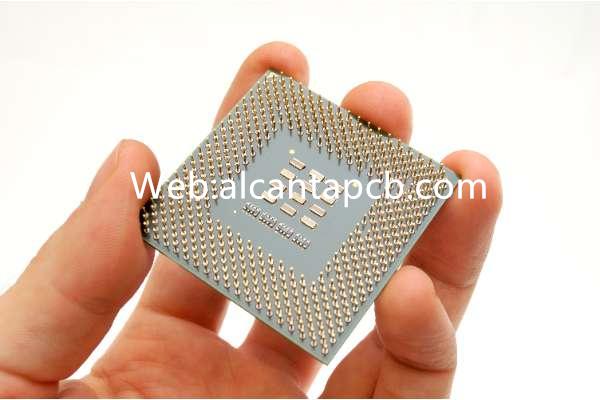
16-I substrati BGA/IC a strati sono circuiti stampati multistrato avanzati (PCB) progettato per ospitare interconnessioni ad alta densità e circuiti complessi per circuiti integrati (circuiti integrati) nella matrice di griglie di sfere (BGA) pacchetti. Questi substrati sono cruciali per i moderni dispositivi elettronici che richiedono potenti capacità di elaborazione, gestione efficiente della potenza, e integrità affidabile del segnale. Poiché i dispositivi elettronici continuano ad evolversi, la richiesta di più strati nei substrati BGA/IC è cresciuta, consentendo maggiori funzionalità e prestazioni in un fattore di forma compatto. Questo articolo esplora le proprietà, struttura, materiali, processo di produzione, applicazioni, e vantaggi dei substrati BGA/IC a 16 strati.
Cos'è un substrato BGA/IC a 16 strati?
Un substrato BGA/IC a 16 strati è un tipo di PCB multistrato dotato di 16 strati distinti di materiali conduttivi e isolanti, che vengono utilizzati per interconnettere i vari componenti di un circuito integrato all'interno di un pacchetto BGA. Questi substrati sono progettati specificamente per supportare progetti elettronici complessi, dove più strati di segnale, aerei di potenza, e i piani di terra sono necessari per gestire l'elevata densità di circuiti e garantire un funzionamento affidabile.
La struttura multistrato consente la separazione di diversi percorsi del segnale, che riduce le interferenze elettromagnetiche (EMI) e diafonia tra i segnali, migliorando così le prestazioni complessive dell'IC. Inoltre, l'uso di più livelli consente l'integrazione di funzionalità avanzate, come i passivi incorporati, che migliorano ulteriormente la funzionalità del substrato.
Struttura di un substrato BGA/IC a 16 strati
La struttura di un substrato BGA/IC a 16 strati è meticolosamente progettata per supportare i complessi requisiti dei moderni circuiti integrati, soprattutto nelle applicazioni ad alte prestazioni. Gli elementi strutturali chiave includono:
Il nucleo del substrato è tipicamente costituito da un materiale dielettrico centrale, come FR-4 o una resina ad alte prestazioni, che fornisce stabilità meccanica e isolamento elettrico. Il nucleo può anche includere componenti incorporati come condensatori o resistori per migliorare la funzionalità.
IL 16 gli strati nel substrato includono più strati di segnale, che sono responsabili del trasporto dei segnali elettrici tra i diversi componenti del circuito integrato. Questi strati sono separati da materiali isolanti per prevenire interferenze del segnale e mantenere l'integrità del segnale.
I piani di alimentazione e di terra sono distribuiti tra gli strati per fornire una distribuzione stabile dell'energia e creare un percorso di ritorno per le correnti elettriche. Questi piani sono essenziali per ridurre al minimo il rumore e garantire il corretto funzionamento dell'IC.
I via sono connessioni verticali che collegano diversi strati del substrato. In un substrato a 16 strati, per collegare i vari strati vengono utilizzati sia vias passanti che microvie, consentendo un instradamento efficiente dei segnali, energia, e collegamenti di terra. Microvie, in particolare, sono fondamentali per mantenere il profilo sottile del substrato garantendo allo stesso tempo interconnessioni affidabili.
Le superfici superiore e inferiore del substrato sono generalmente rifinite con materiali come ENIG (Oro per immersione in nichel chimico) o OSP (Conservante organico di saldabilità) per migliorare la saldabilità e proteggere le tracce di rame sottostanti dall'ossidazione.
Materiali utilizzati nei substrati BGA/IC a 16 strati
I materiali utilizzati nei substrati BGA/IC a 16 strati sono selezionati per la loro capacità di fornire l'energia elettrica necessaria, termico, e le proprietà meccaniche richieste per i circuiti integrati ad alte prestazioni. I materiali chiave includono:
Materiali dielettrici ad alte prestazioni, come FR-4, Resina BT, o resine caricate con ceramica, sono utilizzati per fornire isolamento elettrico tra gli strati. Questi materiali devono offrire costanti dielettriche basse e tangenti a bassa perdita per garantire un'attenuazione minima del segnale e prestazioni ad alta frequenza.
Il rame è il materiale principale utilizzato per gli strati conduttivi nel substrato. Le lamine di rame vengono laminate sottilmente sugli strati dielettrici e quindi modellate per creare le complesse tracce circuitali necessarie per il circuito integrato. La qualità e lo spessore del foglio di rame sono fondamentali per mantenere l'integrità del segnale e garantire prestazioni affidabili.
Materiali adesivi, come il preimpregnato (fibra di vetro preimpregnata), vengono utilizzati per unire insieme i diversi strati. Questi adesivi devono essere selezionati con cura per garantire che forniscano forti legami meccanici mantenendo l'isolamento elettrico e le proprietà termiche del substrato.
La scelta della finitura superficiale, come ENIG o OSP, gioca un ruolo cruciale nell'affidabilità dei giunti di saldatura e nella longevità complessiva del substrato. Queste finiture devono essere compatibili con il passo fine dei pacchetti BGA e fornire un'adeguata protezione contro i fattori ambientali.
Il processo di produzione di substrati BGA/IC a 16 strati
Il processo di produzione dei substrati BGA/IC a 16 strati prevede più passaggi, ognuno di essi richiede precisione e attenzione ai dettagli per garantire che il prodotto finale soddisfi gli elevati standard richiesti per i moderni circuiti integrati. I passaggi chiave includono:
Il processo inizia con la costruzione dei singoli strati. Ogni strato è costituito da un materiale dielettrico laminato con un foglio di rame. La lamina di rame viene quindi incisa per creare lo schema circuitale desiderato, con particolare attenzione alla larghezza e alla spaziatura delle linee per garantire l'integrità del segnale.
Una volta preparati i singoli strati, sono impilati e laminati insieme ad alta pressione e temperatura. Il processo di laminazione deve essere controllato con precisione per garantire che tutti gli strati siano correttamente allineati e che non vi siano sacche d'aria o vuoti che potrebbero influire sulle prestazioni.
I passaggi vengono perforati nella pila laminata per creare connessioni tra gli strati. Queste vie vengono poi placcate con rame per formare i collegamenti elettrici necessari. Microvie, che sono più piccoli e più precisi, sono spesso utilizzati in substrati a 16 strati per mantenere il profilo sottile del substrato.
Il substrato completato viene sottoposto a ispezione e test rigorosi per garantire che soddisfi tutte le specifiche di progettazione. Ciò include il test della continuità elettrica, controllo dell'impedenza, e integrità del segnale. Eventuali difetti rilevati in questa fase possono essere risolti prima che il substrato venga utilizzato nell'assemblaggio del circuito integrato.
La finitura superficiale viene applicata ai cuscinetti di rame esposti per migliorare la saldabilità e proteggere dall'ossidazione. Sul substrato viene quindi applicata una maschera di saldatura per proteggere le tracce del circuito ed evitare ponti di saldatura durante il processo di assemblaggio.
Il substrato finale è sottoposto a un processo completo di controllo della qualità, che include l'ispezione visiva, misurazione dimensionale, e test elettrici. Ciò garantisce che il substrato soddisfi tutti gli standard di prestazioni e affidabilità prima di essere spedito al cliente.
Aree di applicazione dei substrati BGA/IC a 16 strati
16-I substrati BGA/IC a strati sono utilizzati in una varietà di applicazioni elettroniche ad alte prestazioni in cui sono presenti circuiti complessi, elevata integrità del segnale, e una gestione efficiente dell’energia sono necessarie. Le principali aree di applicazione includono:
Nei server, postazioni di lavoro, e altri dispositivi informatici ad alte prestazioni, 16-I substrati BGA/IC a strati supportano i circuiti complessi e ad alta densità richiesti per i processori, moduli di memoria, e altri componenti critici. Gli strati multipli consentono un'efficace distribuzione dell'alimentazione e l'instradamento del segnale in questi ambienti esigenti.
Dispositivi di telecomunicazione, come i router, interruttori, e stazioni base, si affidano a substrati BGA/IC a 16 strati per gestire le elevate velocità di trasmissione dei dati e la complessa elaborazione dei segnali richiesti per le moderne reti di comunicazione. I substrati’ la capacità di supportare circuiti ad alta densità mantenendo l'integrità del segnale è fondamentale per queste applicazioni.
Elettronica di consumo avanzata, compresi gli smartphone, compresse, e console di gioco, utilizzano substrati BGA/IC a 16 strati per far fronte alla crescente complessità dei loro circuiti integrati. Questi substrati consentono ai produttori di racchiudere più funzionalità in fattori di forma più piccoli, migliorare le prestazioni e le capacità di questi dispositivi.
Nelle applicazioni automobilistiche, 16-I substrati BGA/IC sono utilizzati nei sistemi avanzati di assistenza alla guida (ADAS), sistemi di infotainment, e centraline controllo motore (ECU). I substrati’ la capacità di gestire elevati livelli di integrazione e garantire prestazioni affidabili in ambienti difficili è fondamentale per l'elettronica automobilistica.
Vantaggi dei substrati BGA/IC a 16 strati
16-I substrati BGA/IC a strati offrono numerosi vantaggi che li rendono indispensabili per applicazioni elettroniche ad alte prestazioni. Questi vantaggi includono:
Gli strati multipli nei substrati a 16 strati consentono l'integrazione di circuiti complessi e funzionalità avanzate, come i passivi incorporati, in un fattore di forma compatto. Ciò supporta lo sviluppo di circuiti integrati più potenti e capaci senza aumentare le dimensioni del pacchetto.
Fornendo più livelli di segnale e controllando attentamente il posizionamento dei piani di alimentazione e di terra, 16-i substrati a strati aiutano a ridurre al minimo le interferenze elettromagnetiche e la diafonia, garantendo che i segnali vengano trasmessi con alta fedeltà. Ciò è particolarmente importante nelle applicazioni ad alta velocità e ad alta frequenza.
L'inclusione di più piani di alimentazione e di massa consente un'efficace distribuzione dell'energia attraverso l'IC, riducendo il rischio di cadute di tensione e garantendo un funzionamento stabile. Ciò è essenziale per le applicazioni informatiche e di telecomunicazione ad alte prestazioni.
16-I substrati BGA/IC sono progettati per resistere alle sollecitazioni meccaniche, Ciclismo termico, e le condizioni ambientali incontrate nel settore automobilistico, aerospaziale, e applicazioni industriali. La loro struttura robusta garantisce affidabilità a lungo termine anche in condizioni difficili.
Domande frequenti
Perché i substrati BGA/IC a 16 strati sono necessari nel calcolo ad alte prestazioni?
16-I substrati BGA/IC a strati sono necessari nel calcolo ad alte prestazioni perché forniscono le interconnessioni ad alta densità e la gestione avanzata dell'alimentazione necessarie per processori complessi, moduli di memoria, e altri componenti critici. Questi substrati supportano l'integrazione di molteplici funzioni mantenendo l'integrità del segnale e un'efficiente gestione termica.
In che modo i substrati a 16 strati migliorano l'integrità del segnale nelle apparecchiature di telecomunicazione?
16-i substrati a strati migliorano l'integrità del segnale fornendo più strati di segnale e piani di alimentazione e di terra posizionati strategicamente. Ciò riduce al minimo le interferenze elettromagnetiche e la diafonia tra i segnali, garantire che i dati vengano trasmessi con alta fedeltà e bassa latenza nelle apparecchiature di telecomunicazione.
Quali materiali sono comunemente utilizzati nei substrati BGA/IC a 16 strati per l'elettronica di consumo?
Nell'elettronica di consumo, 16-I substrati BGA/IC a strati utilizzano in genere materiali dielettrici ad alte prestazioni come la resina FR-4 o BT, insieme a fogli di rame per gli strati conduttivi. Finiture superficiali come ENIG o OSP vengono applicate per migliorare la saldabilità e proteggere il substrato dai fattori ambientali.
I substrati BGA/IC a 16 strati possono essere utilizzati nelle applicazioni automobilistiche?
SÌ, 16-I substrati BGA/IC a strati sono particolarmente adatti per le applicazioni automobilistiche, compresi i sistemi avanzati di assistenza alla guida (ADAS), sistemi di infotainment, e centraline controllo motore (ECU). La loro struttura robusta e la capacità di gestire circuiti complessi e distribuzione di potenza li rendono ideali per le difficili condizioni dell'elettronica automobilistica.