CO.,LTD")
Produttore di PCB con cavità dell'antenna. Come produttore leader di PCB con cavità dell'antenna, siamo specializzati nella creazione di circuiti stampati ad alte prestazioni progettati per applicazioni di antenne avanzate. La nostra competenza risiede nell’ingegneria di precisione e nei processi produttivi all’avanguardia, garantendo un'integrità ottimale del segnale e interferenze minime. Forniamo soluzioni personalizzate su misura per soddisfare le esigenti esigenze di settori come quello delle telecomunicazioni, aerospaziale, e difesa. Con un impegno per la qualità e l'innovazione, forniamo affidabile, Antenna ad alta frequenza PCB con cavità che garantiscono connettività e prestazioni superiori nei sistemi critici.
PCB con cavità dell'antenna (Circuiti stampati) sono circuiti stampati specializzati progettati per integrare antenne all'interno di una struttura a cavità, ottimizzando le prestazioni di RF (radiofrequenza) e applicazioni a microonde. Questi PCB sono essenziali nelle applicazioni che richiedono la trasmissione di segnali ad alta frequenza, come le telecomunicazioni, aerospaziale, e sistemi di difesa. Questo articolo esplora le caratteristiche, considerazioni di progettazione, materiali, processi di produzione, applicazioni, e vantaggi della cavità dell'antenna PCB.
Cosa sono i PCB con cavità dell'antenna?
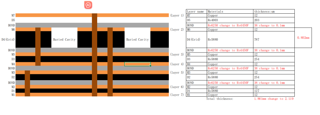
I PCB con cavità dell'antenna incorporano cavità all'interno della struttura del PCB per ospitare le antenne, fornendo un ambiente controllato che migliora le prestazioni del segnale. Queste cavità sono progettate per ottimizzare le proprietà elettromagnetiche, ridurre la perdita di segnale, e migliorare l'efficienza complessiva dell'antenna. L'integrazione delle antenne all'interno della struttura PCB consente progetti compatti ed efficienti, rendendoli adatti per applicazioni ad alta frequenza.
Considerazioni sulla progettazione per PCB con cavità dell'antenna
La progettazione di PCB con cavità d'antenna implica diverse considerazioni critiche:
La forma, misurare, e il posizionamento della cavità sono cruciali per ottimizzare le proprietà elettromagnetiche e le prestazioni dell'antenna.
Scegliere i materiali PCB giusti che offrono una bassa perdita dielettrica, elevata conduttività termica, e prestazioni stabili su tutte le frequenze sono essenziali.
Garantire un corretto adattamento dell'impedenza tra l'antenna e il resto del circuito è vitale per ridurre al minimo la riflessione e la perdita del segnale.
È necessario implementare tecniche efficaci di gestione termica per dissipare il calore generato dai segnali ad alta frequenza.
Sono necessarie tecniche di schermatura adeguate per prevenire le interferenze elettromagnetiche (EMI) e garantire una trasmissione pulita del segnale.
Mantenere tolleranze di produzione strette è fondamentale per garantire prestazioni e affidabilità costanti.
Materiali utilizzati nei PCB con cavità dell'antenna
Diversi materiali sono comunemente usati nella produzione di PCB con cavità d'antenna:
Materiali come Rogers RT/duroid, RO4000, e la serie RO3000 offrono una bassa perdita dielettrica e prestazioni stabili alle alte frequenze.
Questi materiali forniscono eccellenti proprietà termiche ed elettriche, rendendoli adatti per applicazioni ad alta frequenza.
Il rame viene utilizzato per tracce conduttive e pareti di cavità grazie alla sua eccellente conduttività elettrica.
TIM, come grasso termico o pastiglie, sono utilizzati per migliorare il trasferimento di calore tra componenti e soluzioni di raffreddamento.
Materiali conduttivi, come rame o alluminio, sono utilizzati per la schermatura per prevenire le EMI.
Processo di produzione di PCB con cavità d'antenna
Il processo di produzione dei PCB con cavità d'antenna prevede diversi passaggi precisi:
Laminati ad alta frequenza e altri materiali vengono preparati e trasformati in fogli o pellicole.
Le cavità vengono create all'interno degli strati PCB utilizzando precise tecniche di lavorazione o incisione.
Gli strati del PCB, compresa la cavità, sono impilati secondo il disegno, con un'attenta considerazione del posizionamento dei materiali dielettrici e delle tracce conduttive.
Le vie vengono forate e placcate per creare collegamenti elettrici verticali tra i diversi strati e la cavità.
Componenti, compresa l'antenna, sono montati sul PCB utilizzando la tecnologia di montaggio superficiale automatizzata (SMT) processi.
Dissipatori di calore, ventole di raffreddamento, e i materiali dell'interfaccia termica sono integrati per garantire un'efficace gestione termica.
Vengono applicati materiali di schermatura per prevenire le interferenze elettromagnetiche e garantire una trasmissione pulita del segnale.
Le schede assemblate vengono sottoposte a test e ispezioni rigorosi per garantire che soddisfino le specifiche richieste per le prestazioni elettriche, Integrità del segnale, e affidabilità.
Le schede testate e validate vengono assemblate nella loro forma finale, confezionato, e preparato per la distribuzione.
Applicazioni dei PCB con cavità d'antenna
I PCB con cavità d'antenna sono utilizzati in un'ampia gamma di applicazioni ad alta frequenza:
Questi PCB vengono utilizzati nelle stazioni base, antenne, e altri dispositivi di comunicazione in cui la trasmissione del segnale ad alta frequenza è cruciale.
I PCB con cavità d'antenna sono essenziali nei sistemi radar, comunicazione satellitare, ed elettronica militare, dove affidabilità e prestazioni sono fondamentali.
Questi PCB vengono utilizzati nell'imaging medico e nelle apparecchiature diagnostiche che funzionano ad alte frequenze, che richiedono una trasmissione del segnale precisa e affidabile.
I PCB con cavità dell'antenna vengono utilizzati nei sistemi avanzati di assistenza alla guida (ADAS), veicolo-a-tutto (V2X) comunicazione, e sistemi radar.
Questi PCB sono utilizzati nei sensori industriali, sistemi di automazione, e altre applicazioni industriali ad alta frequenza.
Vantaggi dei PCB con cavità dell'antenna
I PCB con cavità d'antenna offrono numerosi vantaggi:
La struttura della cavità riduce al minimo la perdita di segnale e le interferenze, migliorare la potenza e la chiarezza del segnale.
L'integrazione delle antenne all'interno del PCB consente progetti più compatti, risparmiando spazio e riducendo le dimensioni complessive del dispositivo.
L'ambiente controllato della cavità protegge l'antenna dai fattori ambientali, migliorando l’affidabilità e la longevità.
Questi PCB sono progettati per funzionare in modo efficiente alle alte frequenze, rendendoli adatti per applicazioni RF e microonde.
I PCB con cavità d'antenna possono essere personalizzati in base a requisiti specifici, compresa la gamma di frequenza, gestione della potenza, e condizioni ambientali.
Domande frequenti
Quali sono i principali vantaggi derivanti dall'utilizzo di PCB con cavità d'antenna?
I principali vantaggi includono prestazioni del segnale migliorate, design compatto, affidabilità migliorata, capacità ad alta frequenza, e personalizzazione. Questi vantaggi rendono i PCB con cavità d'antenna ideali per applicazioni ad alta frequenza e ad alta potenza.
Quali materiali sono comunemente usati nei PCB con cavità dell'antenna?
I materiali comuni includono laminati ad alta frequenza come Rogers RT/duroid, RO4000, e serie RO3000, PTFE caricato con ceramica, rame per tracce conduttrici e pareti di cavità, materiali di interfaccia termica (TIM), e materiali schermanti come rame o alluminio.
In che modo la progettazione di un PCB con cavità d'antenna garantisce prestazioni elevate?
Il design garantisce prestazioni elevate ottimizzando il design della cavità, selezionando i materiali adeguati, garantire il corretto adattamento dell'impedenza, implementare una gestione termica efficace, applicare adeguate tecniche di schermatura, e mantenendo tolleranze di produzione strette.
Quali sono le applicazioni comuni dei PCB con cavità d'antenna?
Le applicazioni comuni includono le telecomunicazioni (stazioni base, antenne), aerospaziale e della difesa (sistemi radar, comunicazione satellitare), dispositivi medici (imaging medico, diagnostica), Elettronica automobilistica (ADAS, Comunicazione V2X), e applicazioni industriali (sensori, sistemi di automazione). Questi PCB vengono utilizzati in sistemi che richiedono prestazioni ad alta frequenza e trasmissione affidabile del segnale.