CO.,LTD")
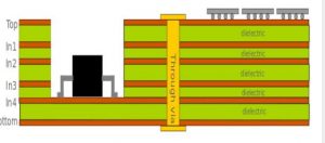
Produttore di PCB a cavità. I PCB a cavità aperta richiedono un ritaglio con profondità controllata per esporre gli strati interni all'aria per l'assemblaggio di antenne o componenti. La fabbrica PCB Alcanta produce molti tipi di schede PCB cavità. Cavità sulle schede PCB. La maggior parte del design. devi mettere qualche IC principale (parti) nelle cavità. SÌ. possiamo produrre questo tipo Pannelli con cavità con alta qualità. possiamo realizzare la cavità del PCB 4 strato a 70 strati. provengono la maggior parte della cavità 4 strato a 16 strati.
In qualche dominio speciale. Il PCB delle cavità utilizzerà materiali PCB ad alta velocità, Materiali PCB ad alta frequenza, Materiali metallici, Materiali FR4 ad alto TG, o altri materiali PCB diversi. possiamo produrre tutti questi tipi di pannelli con cavità di materiali. Alta qualità, e prezzo più conveniente. Quando si progetta questo tipo di cavità PCB. se hai qualche domanda. puoi verificare con noi. ti aiuteremo in qualsiasi momento. non è necessario alcun pagamento. Solo scambio tecnico.

IL Tecnologie PCB delle cavità. SÌ. possiamo realizzare pannelli con cavità con molte tecnologie avanzate. Esempio: Possiamo realizzare il PCB della cavità con Buried e Blind Vias. per favore presta attenzione a sapere. nella zona delle cavità. ci sono alcuni buchi sepolti o ciechi. intendo. i fori di via mostreranno il lato esterno del rame nell'area della cavità.
Informazioni sui materiali dielettrici. se ne hai bisogno. possiamo realizzare il PCB Cavities con molti materiali dielettrici diversi. Piace: Dielettrici di Rogers Dielettrici VS FR4, O, Dielettrici di Rogers VS dielettrici di Isola, Oppure M7, M4, Dielettrici M6, e altro Alte prestazioni, Dielettrici FR4 a bassa perdita. Ditecelo e basta. di che tipo di dielettrici avete bisogno, per favore? ditecelo per favore. possiamo produrlo. e fare un buon lavoro.
Informazioni su altre tecnologie di produzione di PCB con cavità. Piace: Controllo dell'impedenza. possiamo fare +/-5%, Backdrilling, Perforazione e fresatura a profondità controllata, Rigido-flessibile & Circuiti flessibili, e altri. la nostra azienda ha prodotto molti prodotti PCB militari, PCB aeronautico, PCB di comunicazione militare, Prodotto PCB industriale, e molti Prodotti in altri campi.
Altro Ulteriori informazioni sui PCB con cavità: Cos'è il PCB con cavità?
Nel dinamico mondo dell'elettronica, l'innovazione è costante, dando origine a tecnologie specializzate come i PCB con cavità. Questi circuiti stampati esclusivi offrono vantaggi distinti in applicazioni specifiche, rivoluzionando i settori in cui precisione e prestazioni sono fondamentali. Questo articolo approfondisce il concetto di PCB con cavità, facendo luce sulla loro costruzione, applicazioni, e benefici.
Comprendere i PCB con cavità: PCB con cavità, noti anche come PCB con supporto a cavità o schede con cavità, sono un tipo specializzato di circuito stampato caratterizzato da una o più aree incassate, o cavità, lavorato su uno o entrambi i lati. Queste regioni incassate possono variare nella forma, profondità, e dimensioni, a seconda dei requisiti dell'applicazione.
Costruzione di PCB con cavità: La costruzione di PCB con cavità prevede processi tradizionali di fabbricazione di PCB con una fase aggiuntiva: fresatura o fresatura delle cavità sulla superficie della scheda(S). CNC avanzato (Controllo numerico computerizzato) le apparecchiature di lavorazione o fresatura ritagliano con precisione queste cavità, lasciando dietro di sé il substrato che costituisce il fondo o le pareti della cavità. Questo meticoloso processo garantisce l'integrità strutturale soddisfacendo al tempo stesso i requisiti di progettazione specializzati del PCB.
Applicazioni dei PCB con cavità: I PCB con cavità trovano ampio utilizzo in vari settori in cui le prestazioni, affidabilità, e l'integrità del segnale sono fondamentali. Alcune applicazioni importanti includono:
- Sistemi RF e microonde: I PCB con cavità eccellono nelle applicazioni RF e a microonde, in particolare nei sistemi di antenne e nelle apparecchiature di comunicazione. La cavità funge da scudo, riducendo al minimo le interferenze elettromagnetiche e migliorando la trasmissione e la ricezione del segnale.
- Elettronica ad alta frequenza: Nei circuiti ad alta frequenza come i sistemi radar, dispositivi senza fili, e comunicazioni satellitari, I PCB con cavità offrono prestazioni superiori riducendo la perdita di segnale e il rumore, migliorando così l’efficienza complessiva del sistema.
- Aerospaziale e Difesa: I settori aerospaziale e della difesa sfruttano i PCB con cavità in sistemi mission-critical come l'avionica, apparati radar, e sistemi di guida missilistica. Il loro design robusto e l'eccezionale integrità del segnale li rendono indispensabili in questi ambienti esigenti.
- Elettronica medica: Nei dispositivi medici e nelle apparecchiature diagnostiche, I PCB con cavità svolgono un ruolo fondamentale nel garantire letture e diagnosi accurate. La loro capacità di ridurre al minimo le interferenze e mantenere la chiarezza del segnale è preziosa nelle applicazioni mediche sensibili.
Vantaggi dei PCB con cavità: I PCB con cavità offrono numerosi vantaggi chiave, tra cui:
- Integrità del segnale migliorata: Il design della cavità riduce le interferenze elettromagnetiche, con conseguente trasmissione del segnale più pulita e prestazioni complessive migliorate, soprattutto nelle applicazioni ad alta frequenza.
- Gestione termica migliorata: I PCB con cavità facilitano una migliore dissipazione del calore, cruciale per i componenti elettronici che operano in ambienti termici difficili, migliorando così l'affidabilità e la longevità del sistema.
- Ottimizzazione dello spazio: Integrando i componenti all'interno della cavità, I PCB con cavità consentono design compatti e leggeri, rendendoli ideali per applicazioni con spazi limitati in cui dimensioni e peso sono fattori critici.
Conclusione: I PCB con cavità rappresentano una soluzione specializzata su misura per le esigenze uniche dei moderni sistemi elettronici. Con il loro design avanzato, costruzione precisa, e caratteristiche prestazionali superiori, I PCB con cavità continuano a guidare l'innovazione in un'ampia gamma di settori, spingendo i confini di ciò che è possibile nella progettazione e produzione elettronica.
Come progettare un PCB?
Progettare un PCB: Una guida completa:
Progettazione di un circuito stampato (PCB) è una competenza fondamentale sia per gli appassionati di elettronica che per i professionisti. Che tu stia creando un semplice progetto di hobby o un dispositivo elettronico complesso, comprendere il processo di progettazione del PCB è essenziale. Questo articolo fornisce una guida concisa ma completa alla progettazione di un PCB, coprendo i passaggi chiave e le considerazioni lungo il percorso.
Fare un passo 1: Definisci i requisiti Inizia definendo chiaramente i requisiti del tuo PCB. Considera fattori come la dimensione, funzionalità, requisiti di potenza, e le condizioni ambientali in cui opererà. Comprendere questi requisiti in anticipo guiderà l’intero processo di progettazione.
Fare un passo 2: Progettazione schematica Crea un diagramma schematico del tuo circuito utilizzando l'Electronic Design Automation (EDA) software. Questo schema funge da modello per le connessioni tra i componenti e definisce il comportamento elettrico del circuito. Garantire accuratezza e completezza nella fase di progettazione dello schema.
Fare un passo 3: Selezione e posizionamento dei componenti Seleziona i componenti in base alla loro funzionalità, disponibilità, e costo. Una volta scelto, posizionare i componenti sul layout del PCB secondo lo schema. Considera fattori come il routing del segnale, gestione termica, e facilità di assemblaggio durante il posizionamento dei componenti.
Fare un passo 4: Layout PCB Procedere alla fase di layout PCB dopo aver posizionato i componenti. Disporre i componenti sul PCB per ottimizzare l'integrità del segnale, minimize interference, e garantire un routing efficiente. Prestare attenzione a fattori come la lunghezza della traccia, controllo dell'impedenza, e percorsi di ritorno del segnale durante la progettazione del layout.
Fare un passo 5: Instradamento Collegare i componenti sul layout PCB instradando le tracce tra di loro. Seguire le migliori pratiche per l'instradamento delle tracce, come mantenere larghezze di traccia coerenti, evitando spigoli vivi, e minimizzando la diafonia del segnale. Utilizzare piani di terra e di alimentazione per fornire una distribuzione stabile della tensione e ridurre le interferenze elettromagnetiche.
Fare un passo 6: Controllo delle regole di progettazione (Repubblica Democratica del Congo) Esegui un controllo delle regole di progettazione per garantire che il progetto PCB sia conforme ai vincoli di produzione e agli standard di settore. Verificare eventuali violazioni delle autorizzazioni, larghezze minime della traccia, e le dimensioni corrette del cuscinetto. Risolvere eventuali errori o avvisi identificati durante il processo DRC.
Fare un passo 7: Verifica del progetto prima della fabbricazione, verificare la funzionalità e l'integrità del progetto PCB attraverso simulazioni e test. Utilizza software di simulazione per convalidare le prestazioni rispetto alle specifiche di progettazione. Prototipa e testa il PCB per identificare eventuali problemi e apportare le modifiche necessarie.
Fare un passo 8: Genera file di produzione una volta finalizzati e verificati, generare i file di produzione necessari per la fabbricazione. Questi file in genere includono file Gerber per la grafica PCB, lime da trapano per il posizionamento dei fori, e una distinta base (Distinta base) specifiche dettagliate dei componenti. Esaminare la precisione dei file di produzione prima di inviarli al produttore del PCB.
Fare un passo 9: Fabbricazione e assemblaggio Invia i file di produzione a un impianto di fabbricazione PCB per la produzione. Scegli un produttore rispettabile che offra servizi di fabbricazione di qualità. Dopo aver ricevuto i PCB fabbricati, procedere con l'assemblaggio e la saldatura dei componenti secondo la distinta base e le istruzioni di assemblaggio.
Conclusione: Designing a PCB requires careful planning, attenzione ai dettagli, e l’adesione alle migliori pratiche. Seguendo questa guida, puoi creare un PCB ben progettato che soddisfi i requisiti del tuo progetto e funzioni in modo affidabile nell'applicazione prevista. Affina continuamente le tue capacità di progettazione e rimani aggiornato sui progressi della tecnologia PCB per affrontare con sicurezza sfide di progettazione sempre più complesse.
Come produrre un PCB con cavità?
Processo di produzione di PCB con cavità: Una guida completa:
PCB con cavità, noti anche come PCB con supporto a cavità, rappresentano un tipo specializzato di circuito stampato con aree incassate o cavità lavorate su uno o entrambi i lati. Il processo di produzione dei PCB con cavità prevede passaggi unici per ottenere precisione e affidabilità. Questo articolo fornisce una panoramica del processo di produzione, evidenziando i passaggi e le considerazioni principali.
Fare un passo 1: Progettazione e specifiche Il processo di produzione dei PCB con cavità inizia con la fase di progettazione, dove gli ingegneri definiscono il layout, dimensioni, e le specifiche della scheda. Ciò include la determinazione della posizione, misurare, e profondità delle cavità, oltre a selezionare materiali e finiture che soddisfino i requisiti dell'applicazione.
Fare un passo 2: Selezione del materiale La selezione del materiale di substrato appropriato è fondamentale per i PCB con cavità. I materiali comuni includono FR-4, Rogers, e ad alta frequenza laminati, scelto in base a fattori come la costante dielettrica, conduttività termica, e resistenza meccanica. Il materiale del substrato fornisce la base per il PCB e ne influenza le proprietà elettriche e meccaniche.
Fare un passo 3: Lavorazione CNC Una volta finalizzati il design e la selezione dei materiali, il processo di produzione passa al CNC (Controllo numerico computerizzato) lavorazione. Utilizzo di apparecchiature di fresatura o fresatura di precisione, i tecnici ritagliano attentamente le cavità sul substrato PCB secondo le specifiche di progettazione. La lavorazione CNC garantisce precisione e coerenza nelle dimensioni e nel posizionamento della cavità.
Fare un passo 4: Impilamento e laminazione degli strati Dopo la lavorazione delle cavità, il passo successivo è l'impilamento e la laminazione degli strati. Strati multipli di lamina di rame e preimpregnato vengono inseriti tra gli strati del substrato per formare lo stack-up del PCB. Questo accumulo viene quindi pressato insieme ad alta temperatura e pressione utilizzando un processo di laminazione, unendo gli strati in uno unico, struttura coesa.
Fare un passo 5: Foratura e placcatura Una volta laminato lo stack-up del PCB, l'attrezzatura per perforazione di precisione viene utilizzata per creare fori per il montaggio dei componenti e i collegamenti elettrici. Dopo la perforazione, i fori sono placcati in rame per stabilire la conduttività elettrica e garantire interconnessioni affidabili tra gli strati.
Fare un passo 6: Modellazione e incisione dei circuiti La fase successiva prevede la modellazione delle tracce e delle caratteristiche del circuito sugli strati del PCB. Un materiale fotoresist viene applicato alle superfici in rame, seguita dall'esposizione alla luce UV attraverso una fotomaschera, che definisce lo schema circuitale desiderato. Le aree esposte vengono quindi incise tramite soluzioni chimiche, lasciando le tracce e le caratteristiche desiderate del rame.
Fare un passo 7: Finitura superficiale e assemblaggio dopo l'incisione, il PCB è sottoposto a processi di finitura superficiale per proteggere le tracce di rame e migliorare la saldabilità. Le finiture superficiali comuni includono HASL (Livellamento della saldatura ad aria calda), ESSERE D'ACCORDO (Oro per immersione in nichel chimico), e OSP (Conservanti organici di saldabilità). Finalmente, i componenti vengono assemblati sul PCB utilizzando macchine pick-and-place automatizzate, e saldato in posizione utilizzando tecniche di saldatura a riflusso o saldatura ad onda.
Conclusione: Il processo di produzione dei PCB con cavità richiede precisione, competenza, e attenzione ai dettagli in ogni fase. Dalla progettazione e selezione dei materiali alla lavorazione CNC, laminazione, e assemblaggio, ogni fase svolge un ruolo cruciale nella produzione di PCB con cavità di alta qualità che soddisfano i severi requisiti delle moderne applicazioni elettroniche. Seguendo le migliori pratiche e sfruttando tecnologie di produzione avanzate, i produttori possono garantire l'affidabilità e le prestazioni dei PCB con cavità in vari settori.
Possiamo produrre molti tipi di cavità in schede PCB ad alto strato. Se hai domande, non esitate a contattarci con info@alcantapcb.com , Saremo felici di aiutarti.