について 接触 |
電話番号: +86 (0)755-8524-1496
Eメール: info@alcantapcb.com

キャビティ基板 PCB メーカー. High speed and high frequency material cavity 包装基板 and Cavity PCB boards manufacturing. 先進の生産技術.

キャビティ基板 プリント基板, known as such in Chinese, represent a significant advancement in PCB engineering. They feature dedicated cavities within their design, offering an optimal mounting environment for electronic components. This unique structure not only enhances electrical performance by minimizing issues like signal interference and cross-coupling but also improves thermal management capabilities. その結果, these PCBs are crucial components in modern electronic device design.

現代の電子機器では, temperature management has become critical. Cavity Substrate PCBs provide excellent thermal management capabilities through their dedicated cavity design. This structure not only helps dissipate heat, but also effectively isolates heat sources and prevents uneven distribution of temperature on the PCB. したがって, Cavity Substrate PCBs are ideal for reliable operation of electronic components in high temperature environments.

The emergence of Cavity Substrate PCBs marks the field of electronic engineering moving towards higher performance and smaller size. This advanced substrate design not only meets the high performance and high density requirements of modern electronic equipment, but also provides engineers with more innovative possibilities. It is highly adaptable and can take advantage of various application scenarios, thereby promoting continuous innovation in the entire field of electronic engineering.

Cavity Substrate PCBs, as an emerging choice for electronic component assembly, not only represent an important advancement in PCB engineering, but also demonstrate outstanding electrical performance and thermal management. The design of its dedicated cavity provides an ideal mounting platform for modern electronic equipment, bringing more innovation opportunities to engineers. As this technology continues to evolve, we can expect to witness a new era of prosperity in electronic design.

What are the types of Cavity Substrate PCB?

現代の PCB エンジニアリングでは, Cavity Substrate PCBs stand out as a prominent technology due to their adaptability, garnering significant attention in electronic design and manufacturing circles. This article aims to explore various types of Cavity Substrate PCBs, with a particular emphasis on key variants like high-density interconnect (HDI) and rigid-flex combinations. By examining their distinct characteristics in design prerequisites and utilization scenarios, we uncover the diverse applications and requirements of these innovative PCB types.

HDI (高密度相互接続) Cavity Substrate PCBs

Its main feature is its highly integrated interconnect structure, which allows more electronic components to be laid out in a limited space. This allows HDI Cavity Substrate PCBs to exert excellent performance in small electronic devices, providing an ideal solution for mobile devices and smart wearables and other fields.

Rigid-Flex Cavity Substrate PCBs

Rigid-flex cavity substrate PCBs combine rigid and flexible materials, offering designers versatility in creating boards that maintain rigidity in specific sections while allowing flexibility in others. These PCBs find extensive application in electronic devices like foldable mobile phones and wearables that necessitate bending and folding capabilities.

Cavity Substrate PCB Diversity

In addition to the two main types mentioned above, Cavity Substrate PCB technology has also derived many other variants to meet different design needs and application scenarios. These may include customized Cavity Substrate PCBs with special cavity structures for specific industrial applications or electronic equipment in extreme environments.

Different types of Cavity Substrate PCBs are tailored with distinct design features to cater to specific application needs. 例えば, HDI Cavity Substrate PCBs are ideal for compact mobile devices, whereas rigid-flex Cavity Substrate PCBs are suited for electronics demanding flexible designs. The variety in these PCBs mirrors the array of innovative manufacturing technologies employed, such as precision lamination and cavity processing, to guarantee adherence to design and performance specifications.

The variety of Cavity Substrate PCB types reflects the continuous innovation in electronic design and manufacturing. Whether it is meeting high-density interconnect requirements or achieving rigid-flexible designs, Cavity Substrate PCB technology plays a key role in driving breakthroughs in modern electronics. This diversity gives designers more options, allowing them to better adapt to changing market needs.

What are the advantages of using Cavity Substrate PCB?

The emergence of Cavity Substrate PCBs marks a significant leap forward in contemporary electronic design, providing unmatched advantages in electrical functionality, size minimization, そして放熱. These PCBs leverage advanced methods such as high-density interconnect (HDI), delivering accelerated signal transmission rates and minimized distortion. その結果, they are highly sought-after for high-frequency and high-performance tasks, solidifying their position as the premier choice in electronic design.

さらに, Cavity Substrate PCBs facilitate significant miniaturization through innovative manufacturing methods and materials, addressing the challenge of size reduction faced by design engineers. This not only liberates space for device design but also enables electronic products to adapt more flexibly to diverse application scenarios within increasingly compact form factors. 全体, the introduction of Cavity Substrate PCBs has revolutionized electronic engineering, offering unmatched advantages in electrical performance, size efficiency, and thermal regulation.

Cavity Substrate PCBs disperse and conduct heat more efficiently through their unique structure. This is crucial to avoid overheating of electronic components and improve device stability. This advantage makes Cavity Substrate PCBs excellent in high-power, high-density electronic applications.

Designs using Cavity Substrate PCBs have significant advantages in many aspects. This is not only a technical improvement, but also to meet the growing needs of modern electronic equipment. The improvement in electrical performance ensures the reliability of data transmission, the ability to miniaturize makes equipment design more flexible, and excellent thermal management ensures long-term efficient operation of the equipment.

全体, Cavity Substrate PCBs, as a forward-looking technology, brings new possibilities to the design and manufacturing of advanced electronic devices with its excellent performance in electrical performance, miniaturization and thermal management. コミュニケーションの分野であっても、, medical equipment or industrial applications, Cavity Substrate PCBs are gradually becoming the first choice for electronic design engineers, driving the continuous development of electronic engineering.

Why choose Cavity Substrate PCB instead of other boards?

In the dynamic landscape of electronics, Cavity Substrate PCBs have emerged as a frontrunner in electronic design and manufacturing due to their exceptional performance, スペースの効率的な利用, 先進技術との互換性. This choice over traditional PCBs reflects the significant advantages offered by Cavity Substrate PCBs in today’s rapidly evolving industry.

Cavity Substrate PCBs far surpass traditional PCBs in terms of performance. It uses advanced materials and manufacturing technology to provide excellent electrical performance through a dedicated cavity structure. 従来のPCBと比較して, Cavity Substrate PCBs can manage heat more effectively and reduce interference during signal transmission, thereby achieving more stable and reliable electronic performance.

Cavity Substrate PCBs stand out for their compact design and high level of integration. By using high-density interconnect (HDI) テクノロジー, this substrate can accommodate more electronic components in a limited space, thereby achieving miniaturization and lightweight of the device. This excellent space utilization makes Cavity Substrate PCBs ideal for compact designs in modern electronic devices.

In today’s rapidly evolving technological sphere, Cavity Substrate PCBs have surfaced as highly versatile solutions, 驚くべき技術的適応力を示す. 高周波通信などのさまざまな最先端のアプリケーションに合わせてカスタマイズ, 高速データ送信, コンパクトなデザイン, これらの PCB は従来の PCB よりも優れています. 優れた柔軟性により、新興テクノロジーとのシームレスな統合が可能になります。, 将来的には機器のアップグレードが容易になる.

さらに, キャビティ基板 PCB は、性能とスペース利用だけでなく、多層設計でも優れています。. さまざまなレベルで電子コンポーネントを統合することにより、, これらの PCB は信号伝送と熱放散を効率的に管理します。, より信頼性が高く安定した運用環境を確保する.

したがって, 従来の PCB ではなくキャビティ基板 PCB を選択することは、単にトレンドに従うだけではありません, しかし、優れたパフォーマンスを獲得することについては, 優れたスペース利用と先進技術への適応. In electronic design and manufacturing, Cavity Substrate PCBs undoubtedly represent the future, providing strong support for innovation and the realization of superior performance.

What is the method of manufacturing Cavity Substrate PCB?

Cavity Substrate PCBs represent a sophisticated technology in electronic design and manufacturing, characterized by intricate and precise production processes. This article will delve into the manufacturing techniques of Cavity Substrate PCBs, with a primary focus on motherboard and substrate production. It will outline the essential steps, 材料, and highlight the pivotal role of advanced technology in driving this manufacturing process forward.

The subtractive process achieves precise shaping of the motherboard through precise cutting and removal of unnecessary material. アディティブプロセスでは、材料を層ごとに追加して複雑なマザーボード構造を構築します。. これら 2 つのプロセスを組み合わせることで、キャビティ基板 PCB が高精度でカスタマイズ可能になることが保証されます。.

先端材料, 高熱伝導率、高強度基材など, 回路性能と信頼性を向上させるために、キャビティ基板 PCB の製造に広く採用されています。. 同時に, レーザー切断や精密エッチングなどの最先端の製造技術により、マザーボード上の複雑な構造と配線の正確な製造が保証されます。, 電子機器の効率的な機能のための強固な基盤を確立する.
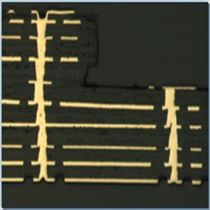
電子部品を収容し保護する構造. High-density interconnection technology realizes tight connections between various electronic components through fine line and through-hole design, improving the integration and performance of circuits.

In the substrate manufacturing of Cavity Substrate PCBs, 素材選びが重要. High-performance materials such as FR-4 and polyimide are widely used with excellent insulation properties and high-temperature stability. While ensuring circuit reliability, they can also effectively withstand working requirements in high-temperature environments, making Cavity Substrate PCBs suitable for various harsh application scenarios.

This thorough examination of motherboard and substrate manufacturing has shed light on the intricate process involved in creating Cavity Substrate PCBs. It underscores the pivotal role played by advanced materials and technologies in this domain. These pioneering manufacturing techniques lay a robust groundwork for enhancing electronic device performance and broadening their application spectrum. With the advent of this new era in Cavity Substrate PCBs, electronic designers and manufacturers are poised to explore wider horizons and unlock fresh possibilities.

What are the applications of Cavity Substrate PCB?

Cavity Substrate PCBs are at the forefront of electronic engineering today, proving indispensable across industries due to their exceptional design and adaptability. From aerospace to telecommunications and medical devices, these advanced substrates are widely utilized, showcasing their versatility and essential role in cutting-edge electronic designs.

航空宇宙分野, Cavity Substrate PCBs are crucial for both aircraft and spacecraft. Their lightweight construction and high-density interconnections make them perfect for avionics systems. Their extensive use in navigation, コミュニケーション, and control systems significantly enhances overall system performance and reliability.

In the rapidly developing communications industry, Cavity Substrate PCBs have become the core of modern communications equipment. Its highly integrated nature allows it to play a key role in wireless base stations, communication network equipment and satellite communication systems. These substrates facilitate advancements in communications technology by providing superior signal transmission and processing performance.

Cavity Substrate PCBs are increasingly integral in diverse industries such as medical device manufacturing, 産業用自動化, and automotive engineering. これらの基板, known for their customizability and reliability, serve critical functions in complex equipment like medical imaging devices, 産業用制御システム, and vehicle electronics. Their ability to withstand high temperatures and offer high density makes them ideal for demanding environments. By enhancing electronic equipment performance and reliability, these substrates drive innovation across various sectors, catering to unique industry requirements and accelerating technological advancement.

Where to find Cavity Substrate PCB?

In today’s electronic engineering landscape, the demand for high-performance Cavity Substrate PCBs is on the rise. These specialized components offer superior characteristics vital for modern design and manufacturing processes. しかし, finding reliable and top-quality Cavity Substrate PCBs in the expansive market can pose a significant challenge for engineers and decision-makers alike. This article aims to offer guidance on effectively sourcing these advanced electronic engineering tools, 読者が自分のプロジェクトについて十分な情報に基づいた決定を下せるようにする.

専門的な専門知識:With extensive professional experience, we stand as leaders in the field, comprehensively understanding the design and manufacturing intricacies of Cavity Substrate PCBs to address diverse project requirements effectively.

先進技術:We employ cutting-edge manufacturing technologies, including High Density Interconnect (HDI), to elevate the performance and reliability of our Cavity Substrate PCBs to optimal levels.

品質保証:Our stringent quality control practices span from raw material procurement through production to final delivery, ensuring that each Cavity Substrate PCB adheres to uncompromising quality standards.

カスタマイズ:We offer flexible customization services tailored to meet the specific needs of our customers, ensuring seamless integration with varying project requirements.

If you are seeking a dependable Cavity Substrate PCB supplier, we warmly invite you to connect with us. Partnering with us guarantees access to high-quality products, expert technical support, and the adaptability needed to address your project demands effectively. For more information about our offerings, please visit our official website [Company Website Link].

In the expansive electronic engineering market, selecting the right Cavity Substrate PCB supplier is paramount. By choosing a reputable manufacturer like us, you not only secure top-notch products but also gain professional assistance to drive the success of your projects. We eagerly anticipate collaborating with you to advance innovation in electronic engineering.

What is the quote for Cavity Substrate PCB?

The pricing of Cavity Substrate PCBs in modern electronics manufacturing is a crucial aspect for potential adopters to consider for project success. This article delves into the intricacies of Cavity Substrate PCB quotations, shedding light on the various cost considerations and influencing factors.

The cost of Cavity Substrate PCBs is more than just a figure; it embodies the intricate manufacturing complexity and technological advancements. Understanding key factors is paramount to grasping how quotations are formed:

Diverse Types of Cavity Substrate PCBs:Various types of Cavity Substrate PCBs may necessitate distinct materials and processes throughout manufacturing. Utilizing specialized substrates like high-density interconnect (HDI) or rigid-flex can lead to increased manufacturing expenses.

The core feature of Cavity Substrate PCBs is their dedicated cavities. The design specifications of the cavity, such as depth, shape and layout, will directly affect the difficulty and cost of manufacturing.

Mass production often reduces manufacturing costs per unit. Large-scale orders may enable manufacturers to utilize resources more efficiently and thus provide more competitive quotes.

The manufacturing of Cavity Substrate PCB involves high-performance materials such as high-temperature-resistant polyimide. These specialty materials are often more expensive, directly affecting the overall cost.

The manufacturing of Cavity Substrate PCB requires complex processes including precision cutting, drilling and inter-layer connections. These high-precision processes increase production costs.

The latest technology and equipment used by manufacturers will directly affect costs. Advanced manufacturing technologies may increase efficiency, but may also require higher investments.

Quotations for Cavity Substrate PCB are flexible and vary based on the needs of the specific project. To provide potential adopters with a comprehensive understanding, manufacturers will often provide customized quotes that take into account the project’s unique requirements and volume production plans.

When selecting Cavity Substrate PCB, potential adopters should fully understand these cost factors in order to make an informed decision. Investing in high-performance Cavity Substrate PCBs may provide long-term competitive advantages for future electronic products.

In the complex field of electronics manufacturing, an in-depth understanding of the Cavity Substrate PCB quote is the first step in ensuring project success. By understanding its manufacturing process, cost considerations and influencing factors, potential adopters can better plan and optimize their electronic designs towards a future of innovation and excellence.

Cavity Substrate PCB

Common problem

What advantages do Cavity Substrate PCBs offer over traditional boards?

Cavity Substrate PCBs boast advantages such as improved electrical performance, 小型化能力, 優れた熱管理. These features make them preferable for cutting-edge electronic devices seeking optimal efficiency.

What customization options are available for Cavity Substrate PCBs?

Cavity Substrate PCBs offer customization options to meet specific design requirements. These may include variations in cavity dimensions, 基板材料, and other parameters to align with the unique needs of electronic devices.

Are Cavity Substrate PCBs compatible with existing electronic components and technologies?

Cavity Substrate PCBs are designed with compatibility in mind. They can seamlessly integrate with existing electronic components and technologies, providing a forward-looking solution for evolving electronic designs.

What distinguishes Cavity Substrate PCBs from traditional PCBs?

Cavity Substrate PCBs stand out due to their specialized design featuring enhanced electrical and thermal performance. 従来のPCBとは異なり, they incorporate dedicated cavities for optimized component placement and connectivity.

What advantages do Cavity Substrate PCBs offer?

Cavity Substrate PCBs boast advantages such as improved electrical performance, 小型化能力, 優れた熱管理. These attributes make them a preferred choice for advanced electronic devices.

How does the manufacturing process of Cavity Substrate PCBs differ from traditional PCBs?

The manufacturing process involves specialized steps for creating dedicated cavities and high-density interconnects. Both motherboard and substrate production utilize subtractive and additive manufacturing processes with advanced materials and technologies.

Can Cavity Substrate PCBs be customized for specific applications?

確かに, Cavity Substrate PCBs offer customization options to meet specific design and application needs. The ability to tailor these PCBs to unique requirements makes them adaptable to diverse electronic projects.

Are there compatibility considerations when integrating Cavity Substrate PCBs into existing designs?

Compatibility considerations depend on the specific requirements of the project. しかし, Cavity Substrate PCBs are designed to be adaptable, and manufacturers can provide guidance on integration compatibility.

前へ:

次:

返信を残す

このサイトはスパムを低減するために Akismet を使っています. コメントデータがどのように処理されるかをご覧ください.