株式会社")
セラミック基板とパッケージ。高速・高周波材料パッケージ基板の製造. 先進的なパッケージ基板の製造プロセスと技術.
セラミックス, もろさや芸術的な職人技と関連付けられることが多い, 実はエレクトロニクスの分野で極めて重要な位置を占めている. 装飾的な側面を超えて, セラミックスは、さまざまな電子用途に不可欠なコンポーネントとして機能します. この記事では、セラミック基板とパッケージの領域についての啓発的な探求を提供します。, さまざまな電子分野で広く使用されています. 私たちの現代世界では, 電子機器は日常生活にシームレスに組み込まれています, スマートフォンにまたがる, 自動車制御システム, 通信機器, および医療機器. この広大で複雑な風景の中で, セラミックスは欠かせない素材として登場, その独特の特性と特質により、電子機器製造における最優先の選択肢としての地位を確立しています。.
セラミックは高温での優れた安定性で高く評価されています, 絶縁特性, 機械的堅牢性, および化学的不活性性. これらの特性により、セラミックは電子部品にとって理想的な選択肢となります。, 特に高温を特徴とする厳しい環境では, 周波数, そしてプレッシャー. セラミックの絶縁能力は、電子部品間の干渉を防ぐのに役立ちます。, これにより、回路の安定性と全体的なパフォーマンスが向上します。.
さらに, 極端な温度と周波数条件下で動作するように設計された電子機器において、セラミックパッケージがどのように役立つかを調査します。. テクノロジーが絶え間なく進化を続ける中、, セラミックスの応用範囲は広がり続ける. この記事は、この魅力的な領域への入り口として機能します, セラミックスがエレクトロニクス業界内でイノベーションと進歩をどのように推進するかについての洞察を提供します.
この記事を読み進めていくと、, 陶芸への理解を深めることができます’ エレクトロニクス分野の中心的な重要性を学び、エレクトロニクス分野の進歩におけるイノベーションと持続可能な実践の重要な役割についての認識を養います。. 陶芸の世界への探検に参加し、その無限の可能性を発見してください。.
セラミック基板の電子分野への応用
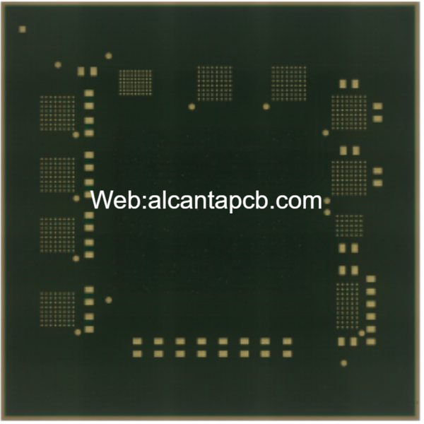
セラミック基板はエレクトロニクスの分野で極めて重要な技術を代表します. その独特の構造と特性により、それらは多数の電子機器に不可欠な要素となっています。. このセグメントでは, 私たちはセラミック基板を支える基本原理の広範な探求に着手します。, エレクトロニクス製造の状況に対する彼らの重要な貢献, そして実際のアプリケーションについて詳しく見ていきます, のようなインスタンスを含む プリント基板 (プリント基板) とセンサー.
セラミック基板の基本概念と構造
セラミック基板は通常、酸化アルミニウムなどの絶縁セラミック材料から作られます。 (Al2O3) または窒化ケイ素 (Si3N4). その構造には通常、特殊な接着剤と製造プロセスを通じて複雑に結合された複数のセラミック層が含まれます。. この多層アーキテクチャは電子アプリケーションで重要な役割を果たします, 電気的絶縁を提供するだけでなく、優れた熱伝導性を備え、優れた機械的堅牢性を示します。.
電子製造におけるセラミック基板の重要な役割
セラミック基板はエレクトロニクス製造の現場に不可欠です. さまざまな電子コンポーネントのサポートおよび相互接続に幅広く使用されています。, 集積回路を含む, 抵抗器, コンデンサ, その他さまざまな要素. これらの基板は、これらのコンポーネントの取り付けと接続のための頑丈なプラットフォームを提供します。, 最適な機能を確保する.
さらに, セラミック基板は熱伝導と放熱に優れています. 熱を周囲環境に効率的に伝達します。, 電子機器の安定した性能維持に貢献します。. この機能は、高出力電子アプリケーションにおいて特に重要です。, パワーモジュールやアンプなど.
プリント基板 (プリント基板): PCB製造の分野で, セラミック基板が重要な役割を担う. PCB の基礎基板として機能します。, 電気絶縁性と熱伝導性の両方を実現. この構成は、高周波エレクトロニクスに特に適しています。, 通信機器と無線周波数で証明されるように (RF) アプリケーション.
センサー: セラミック基板はセンサー技術で広く応用されています. 例えば, 高温高圧環境では、シェル圧力センサーのセラミック基板を利用して圧力変化を測定します. セラミック基板の絶縁性と熱伝導性により、さまざまなセンサーに最適です。, 温度センサーを含む, 加速度計, およびガスセンサー.
本質的には, セラミック基板は電子製造の分野でかけがえのない役割を果たしています. 独特の構造と特性により、さまざまな用途に適しています。, PCB からセンサーに至るまで、また高周波エレクトロニクスから高温高圧条件によってもたらされる課題に至るまで、. これらの基板は、現代の電子技術の進化にとって重要な原動力として機能します。, イノベーションと持続可能な慣行の採用のための強固な基盤を提供する.
エレクトロニクス分野におけるセラミックパッケージングの重要性
セラミックパッケージングは、カプセル化に広く採用されている技術です。 半導体チップ 各種電子部品や. 複数の重要な機能を果たします, その主な役割の 1 つは機械的保護です。. 電子機器は、多くの場合、さまざまな環境および運用上の課題に直面します。, 振動も含めて, 衝撃, そして気温の変動. セラミック パッケージの固有の硬度と弾力性により、半導体チップに最適なシールドが提供されます。. さらに, セラミックパッケージは埃に対するバリアとして機能します, 水分, およびその他の汚染物質, デバイスの寿命を効果的に延長します.
さらに, セラミックパッケージは、エレクトロニクス分野での電気絶縁を確保する上で極めて重要な役割を果たします. セラミック材料は本質的に絶縁特性を持っています, これにより、望ましくない電流の流れが防止されます。. この絶縁は、電子機器の安全かつ信頼性の高い動作の基礎となります。, 特に高電圧を必要とするアプリケーションでは, パワーエレクトロニクスなど.
加えて, セラミックパッケージは光周波数と無線周波数を保護する上で重要な役割を果たします (RF) コンポーネント. 光学センサーと高周波 RF コンポーネントは、多くの場合、そのパフォーマンスを確保するために特定の環境を必要とします。. セラミック材料は、光学性能や高周波電気信号の伝送にほとんど影響を与えないため、これらの用途に優れています。, 機械的保護と電気絶縁を提供しながら.
高温および高周波アプリケーションにおける利点について説明する
セラミックパッケージは、高温および高周波用途において明確な利点をもたらします。, エレクトロニクスの分野で重要なコンポーネントとなっています. セラミック材料は極端な温度条件下でも顕著な安定性を示します, 高温環境でのアプリケーションにとって重要な特性, 宇宙船も含めて, 自動車エンジン制御モジュール, およびパワーエレクトロニクス機器. さらに, 陶器’ 誘電率が低いため、高周波回路にとって理想的な選択肢となります。, 電磁放射の吸収が最小限に抑えられ、優れた絶縁特性を示すためです。.
まとめると, エレクトロニクス分野におけるセラミックパッケージングの重要性は、いくら強調してもしすぎることはありません。. 機械的保護と電気絶縁を提供するだけでなく、高温および高周波シナリオにおいて比類のない強度を誇ります。. これにより、セラミックパッケージが現代のさまざまな電子アプリケーションの中心に据えられます。, エレクトロニクス分野で絶え間ない革新と進歩を推進.

電子応用におけるセラミックスの多様性
セラミックは、その多くの種類と特性でエレクトロニクス分野で知られています。, 酸化アルミニウムと窒化ケイ素の 2 つの主なタイプ. これらのセラミック材料は、電子用途で特定の用途に使用されます。, さまざまな業界に主要なソリューションを提供する.
アルミナセラミック
アルミナセラミックス, 単にアルミナと呼ばれることが多い, 優れた絶縁性と優れた耐熱性で知られる特徴的なセラミック素材として注目されています。. 電子アプリケーションの分野では, その主要な属性には以下が含まれます:
絶縁特性: アルミナセラミックスは絶縁体として優れています, 電子部品の絶縁と絶縁に最適な選択肢です。. 電子回路内の絶縁体としての用途が見つかります。, デリケートなコンポーネントの確実な分離と保護.
高温耐性: 高温環境下でも優れた弾力性を誇るセラミック素材, 高温にさらされる電子アプリケーションにとって非常に価値のあるものになります。. アルミナセラミックは、高温の電子領域で特に有益であることが証明されています, パワーモジュールやパワー半導体を含む, 耐熱性が重要な資産となる場合.
硬度: アルミナセラミックスは硬度が高く、耐摩耗性に優れた電子部品です。, 電子機器の端子台やコネクタなど.
窒化ケイ素セラミックス
窒化ケイ素セラミックは、さまざまな電子用途における多用途な特性が評価され、さらに普及しているセラミック材料です。. これらの属性には次のものが含まれます:
熱伝導率:優れた熱伝導率を誇る窒化ケイ素セラミックス, 高出力電子部品に最適です。, 特にパワー半導体デバイスの分野では.
耐薬品性:このセラミック材料は化学的腐食に対して顕著な耐性を示します。, 困難な環境におけるアプリケーションにとって信頼できる選択肢となる, 化学装置内の電子センサーなど.
絶縁:窒化ケイ素セラミックスは効果的な絶縁材料として機能します, 高電圧用途に最適に調整, 高圧電力設備を含む.
電子用途における酸化アルミニウムおよび窒化ケイ素セラミックの特性により、これらは、多様な電子デバイスの特有の要件を満たすよう努める設計エンジニアにとっての主要な選択肢となります。. これらの材料の多様性と多用途性は、エレクトロニクス産業をサポートする上で極めて重要な役割を果たします。, 進化するニーズに適応し、電子技術の絶え間ない進歩を促進できるようにする.
セラミック応用分野の今後の動向
エレクトロニクスの分野では, セラミック用途は進化の過程を続けています, 現代のテクノロジーの需要に対応する準備ができています. この開発の軌跡には、技術革新が含まれるだけでなく、持続可能性と環境保護もますます重視されています。.
進化を続けるセラミック技術を探る
この進歩により、エレクトロニクスの分野での広範な利用の可能性が広がりました。. 例えば, 窒化ホウ素セラミックは、高出力半導体パッケージングの主な選択肢として浮上しています, 高温および高周波数での優れた性能により、.
さらに, セラミックス材料の微細加工技術は常に進化を続けています. 微細加工の進歩, 3D印刷, およびその他の製造技術により、セラミック部品の精密製造に新たな機会がもたらされています。. この軌跡は、より小規模なシステムの統合が期待できることを示唆しています。, 電子機器の複雑なデザインのセラミック部品, これにより、全体的なパフォーマンスと信頼性が向上します。.
持続可能性と環境トレンドを重視
持続可能な開発が求められる今日の時代に, セラミックスは環境に優しいという理由で広く注目を集めています. 従来のプラスチックや金属と比較した場合, セラミックは、製造時と使用時の両方で汚染が少ないという利点を誇ります。, 長い耐用年数を享受する, 高温環境でも堅牢な性能を発揮. これらの特性が総合的に電子機器のエネルギー消費量の削減に貢献します。.
将来を見据えて, エレクトロニクス製造業界が持続可能なソリューションを追求し続ける中、, セラミックは、好ましい材料の選択肢として浮上する準備ができています. セラミックスは、その優れた絶縁特性により、電気自動車や再生可能エネルギー技術において極めて重要な役割を果たします。, 電池や電子機器の効率向上が期待されている場合.
結論は, セラミック応用の将来には、豊富な機会と課題が潜んでいます. テクノロジーの進歩により、エレクトロニクス分野におけるセラミック材料の独創的な応用が促進される, 一方、持続可能性と環境保護のトレンドに鋭い注目を集めることで、エレクトロニクス産業はより環境に優しく効率的な軌道に向かって推進されるでしょう。. 基礎材料として, セラミックスは今後も中心的な役割を果たし続ける, エレクトロニクス分野の革新と進歩を推進.
エレクトロニクス領域内, セラミックスの重要性を過小評価することはできません. セラミック基板からセラミックパッケージまで, これらは電子アプリケーションにおいて極めて重要な役割を果たし、現代のテクノロジーの進化に実質的なサポートを提供します。.
エレクトロニクスにおけるセラミックスの重要な役割
セラミック基板, プリント基板内の統合コンポーネントとして機能する (プリント基板), 電子機器に安定した機械的サポートと優れた電気的性能を提供します。. 高い絶縁性と優れた耐熱性により、セラミック基板は高周波電子機器に特に適しています。, マイクロ波通信装置や高周波回路など. さらに, セラミック基板はセンサー技術において極めて重要な役割を担う, 温度などのパラメータの測定を容易にする, プレッシャー, 湿度と, それにより、さまざまな業界に正確なデータを提供します.
梱包に関しては, セラミック材料の低い熱膨張係数と優れた熱伝導性により、セラミック材料は高出力電子デバイスに最適な選択肢となります。. セラミックパッケージは熱を効率的に放散するだけでなく、最も厳しい温度条件下でも電子部品の性能を維持します。. この機能は軍事用途には不可欠であることが証明されています, 航空宇宙, およびエネルギー部門.
私たちは、エレクトロニクスの分野におけるセラミックスの革新的な用途の継続的な探求を提唱します。. 電子技術が進歩するにつれて, パフォーマンスの向上に対する要求, 縮小サイズ, 信頼性の向上はますます高まり続けています. セラミック材料は、これらの急成長する要件に適切に対応できる独自の特性を備えています。, 新たな応用領域を積極的に模索する必要性を強調.
さらに, セラミックスの持続可能な特性と環境上の利点により、セラミックスは今後の電子用途における環境に優しい材料の選択肢として位置付けられます。.
総括する, エレクトロニクス分野で欠かせないセラミックス. 基板や包装材料として機能します。, 電子機器に信頼性の高い性能と高い安定性を提供します。. テクノロジーが進化し続けるにつれて, 私たちはエレクトロニクス分野の進歩を促進するために、エレクトロニクス用途におけるセラミックスの革新的な使用法を模索し続ける必要があります。, 技術開発と環境保護が相互に補完し合うよう、持続可能な実践に焦点を当てながら. これは、よりスマートなシステムの構築に役立ちます, より効率的で環境に優しい未来.