株式会社")
CPUボールパッケージ基板メーカー。CPUボールのリーディングカンパニーとして パッケージ基板 メーカー, 当社は、高度なコンピューティング アプリケーションに最適なパフォーマンスと信頼性を保証する高品質の基板の製造を専門としています。. 当社の最先端の製造プロセスと厳格な品質管理により、最高の業界基準を満たす基板が保証されます。, 最新の CPU の厳しいニーズに応える.
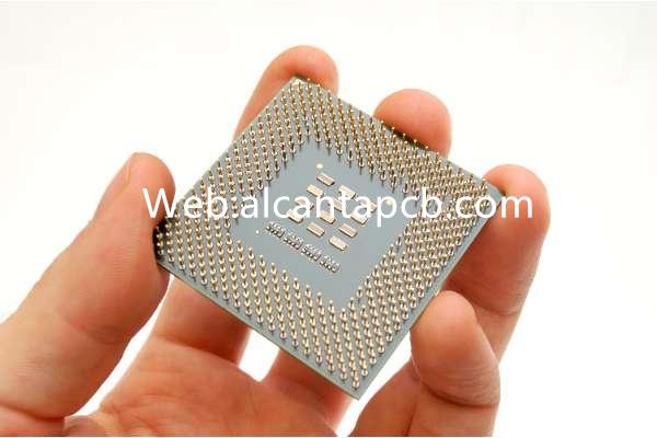
CPU ボール パッケージ基板は、最新の中央処理装置の構築における重要なコンポーネントです。 (CPU). これらの基板は、半導体ダイが取り付けられ、電子システムの残りの部分に接続される基礎層として機能します。. これらは電気的な安全性を確保する上で重要な役割を果たします。, 熱, CPU の機械的性能, 特に高性能コンピューティング環境では.
CPUボールパッケージ基板とは?
CPUボールパッケージ基板はパッケージの一種です 基板 中央処理装置専用に設計. 通常、CPU ダイをシステムの他の部分に取り付けて相互接続するためのプラットフォームを形成する複数の絶縁材料と導電材料の層で構成されています。. の “ボール” この名前は、基板の下側にあるはんだボールの配列を指します。, マザーボードへの電気接続を容易にする.
多層構造: 電気信号のルーティングを提供する誘電体と導電性材料の複数の層で構成されています。.
はんだボール: マザーボードに接続する基板の下側のはんだボールの配列, 堅牢な電気接続を確保する.
熱管理: CPU から発生する熱を効果的に放散する先進的な素材と設計.
CPUボールパッケージ基板のデザインリファレンスガイド
CPU ボール パッケージ基板の設計には、最新の CPU のパフォーマンスと信頼性の要件を確実に満たすために、いくつかの重要な考慮事項が含まれます。.
適切な材料を選択することは、パフォーマンスと信頼性にとって非常に重要です. 一般的な資料には含まれます:
BTレジン (ビスマレイミド トリアジン): 優れた電気絶縁性と熱安定性を実現.
ポリイミド: 高温耐性と機械的強度で知られています.
銅: 優れた導電性により、導電性トレースやパッドに使用されます。.
CPU ボール パッケージの基板は通常、複数の層で構成されています, 含む:
コア層: 構造的完全性を提供する中央絶縁層.
ビルドアップ層: 配線密度を高め、電気的性能を向上させるためにコアに追加された層.
表層: マザーボードに接続するためのはんだボールを含む最外層.
CPU のパフォーマンスと寿命を維持するには、効果的な熱管理が不可欠です. テクニックとしては、:
サーマルビア: ダイからヒートシンクに熱を伝達する伝導経路.
ヒートスプレッダー: 熱の分散と放散を助ける金属層またはコンポーネント.
サーマルインターフェースマテリアル (ティム): 熱伝導率を高めるためにダイとヒートスプレッダーの間に材料を配置.
電気的性能を確保するには、制御されたインピーダンスを維持する必要があります, 信号損失を最小限に抑える, クロストークの低減. これには必要です:
高精度のトレースルーティング: インピーダンスを制御するための配線幅と間隔の慎重な設計.
グランドプレーン: ノイズを低減し、信号の完全性を向上させるための接地専用の層.
シールド: 敏感な信号を電磁干渉からシールドする技術.
CPUボールパッケージ基板に使用されている材料?
CPU ボール パッケージ基板に使用される材料は、電気的特性を考慮して選択されています。, 熱, および機械的特性. 一般的な資料には含まれます:
BTレジン: 優れた電気絶縁性と熱安定性で知られています, BT 樹脂は基板コアとして一般的な選択肢です.
ポリイミド: 高温耐性と機械的強度に優れた高性能ポリマーです。, 高度な電子アプリケーションに適したものになります.
銅: 導電性トレースとパッドに不可欠, 銅は優れた導電性を備え、ビルドアップ層と表面層に広く使用されています。.
セラミックス材料: 優れた熱伝導性と安定性のために使用されることもあります, アルミナや窒化アルミニウムなどのセラミックは、基板の熱管理機能を強化できます。.
はんだボール: 通常は鉛フリーはんだ合金で作られています, これらのボールは、基板とマザーボード間の電気的および機械的接続を提供します。.
CPUボールパッケージ基板のサイズはどれくらいですか?
CPU ボール パッケージ基板のサイズは、特定の CPU とその用途に応じて大きく異なります。. サイズに影響を与える要因には次のものがあります。:
ダイサイズとピン数: CPU ダイのサイズと必要な接続の数は、基板全体のサイズに影響します。. より大きなダイとより多くのピンを備えた高性能 CPU には、通常、より大きな基板が必要です.
申請要件: さまざまなアプリケーション, デスクトップなどの, サーバ, またはモバイルCPU, 基板サイズに影響を与えるさまざまなサイズ制約と性能要件がある.
製造基準: 業界標準と製造能力も、CPU ボール パッケージ基板のサイズを決定する役割を果たします。. 標準サイズはありますが、, 特定の用途向けにカスタム サイズを設計できる.
CPUボールパッケージ基板の製造工程
CPU ボール パッケージ基板の製造プロセスには、正確に制御されたいくつかのステップが含まれます:
CAD設計: 詳細なCADモデルが作成されます, すべてのレイヤーを組み込む, 痕跡, およびコンポーネント.
シミュレーション: 設計を最適化し、性能要件を満たしていることを確認するために、電磁シミュレーションと熱シミュレーションが実行されます。.
ラミネーション: 絶縁材料と導電材料の複数の層が積層されて基板が形成されます。.
穴あけ加工とメッキ加工: 電気接続を確立するために、層にビアが開けられ、銅でメッキされます。.
フォトエッチング: 回路パターンはフォトエッチング技術を使用して基板に転写されます, フォトレジストの塗布を伴う, マスク越しに紫外線を当てると, 保護されていない領域をエッチングして除去します.
メッキ: 電気的性能を向上させるために、導電性トレースとパッドに追加の銅メッキが施されています。.
はんだボールの配置: はんだボールは自動化装置を使用して基板の下面に正確に配置されます.
リフローはんだ付け: 基板はリフローはんだ付けされ、はんだボールが溶けて固まります。, 堅牢な電気的および機械的接続を作成する.
電気試験: すべての接続に損傷がなく、基板が意図したとおりに機能することを確認するために、厳格な電気テストが実施されます。.
熱試験: 熱試験では、基板の熱を放散し、動作条件下で性能を維持する能力を検証します。.
最終検査: 徹底した検査により、基板がすべての設計仕様と品質基準を満たしていることが確認されます。.
CPUボールパッケージ基板の応用分野
CPU ボール パッケージ基板は、高性能と信頼性が重要なさまざまなアプリケーションで使用されます。:
家電: デスクトップおよびラップトップの CPU で使用される, これらの基板は、日常のデバイスでのハイパフォーマンス コンピューティングをサポートします。.
データセンターとサーバー: 高性能 CPU 基板はサーバーおよびデータセンター アプリケーションに不可欠です, 信頼性とパフォーマンスが重要な場合.
モバイルデバイス: スマートフォンやタブレットでは、高性能モバイル コンピューティングをサポートするために、より小型で効率的な CPU 基板が使用されています。.
組み込みシステム: これらの基板は組み込みシステムにも使用されています, 産業用の処理能力を提供, 自動車, およびIoTアプリケーション.
高性能コンピューティング (HPC): HPC システムで使用される, これらの基板は、最も要求の厳しい計算タスクをサポートします。, 科学シミュレーションやデータ解析など.
CPUボールパッケージ基板のメリットとは?
CPU ボール パッケージ基板には、高性能コンピューティング アプリケーションに適したいくつかの利点があります。:
電気性能の向上: 多層設計と正確な配線により、優れた電気的性能を保証します, 信号損失とクロストークの最小化.
強化された熱管理: 先進的な素材と熱管理技術により、熱を効果的に放散します。, CPUのパフォーマンスと信頼性を維持する.
コンパクトで効率的な設計: はんだボールと埋め込みコンポーネントの使用により、よりコンパクトで効率的な設計が可能になります。, マザーボード上のスペースを節約する.
耐久性と信頼性: 高品質の素材と厳格な製造プロセスにより、これらの基板の耐久性と信頼性が保証されます。, 厳しい条件下でも.
カスタマイズ性: カスタム設計を作成できるため、特定のアプリケーション要件を満たすカスタマイズされたソリューションが可能になります, 最適なパフォーマンスを確保する.
よくある質問
ハイパフォーマンス コンピューティングで CPU ボール パッケージ基板を使用する主な利点は何ですか??
CPU ボール パッケージ基板により電気的性能が向上, 強化された熱管理, コンパクトで効率的な設計, 耐久性, 信頼性, そしてカスタマイズ性, ハイパフォーマンス コンピューティング アプリケーションに最適です。.
はんだボールはどのようにしてCPUボールパッケージ基板に取り付けられるのか?
自動化装置を使用してはんだボールを基板の下側に配置し、リフローはんだ付けして堅牢な電気的および機械的接続を作成します。.
CPUボールパッケージ基板に一般的に使用される材料は何ですか?
一般的な材料にはBT樹脂が含まれます, ポリイミド, 銅, 陶器, および鉛フリーはんだ合金.
CPUボールパッケージ基板はどの業界で最もよく使用されていますか?
CPU ボール パッケージ基板は家庭用電化製品で一般的に使用されています, データセンターとサーバー, モバイルデバイス, 組み込みシステム, および高性能コンピューティング.
CPU ボール パッケージ基板は熱管理をどのように改善するのか?
CPU ボール パッケージ基板はサーマル ビアの使用により熱管理を改善します, ヒートスプレッダ, 放熱性を高めCPU性能を維持する高性能素材を採用.