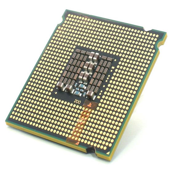
fcbga-package&fcbga-substrate
FCBGA package&FCBGA Substrate Vender,Flip-chip package substrate, we have made the ball Pitch 100um(4mil). laser via drill size 50um(2 mil). and 25um(1mil) for the laser via copper ring. the best samllest pads to pads gap are 9um(1.2mil). Advanced FCBGA package substrate technology.
Improve electrical performance and incorporate higher IC functionality: Alcanta Flip Chip BGA (FCBGA) packages are assembled around state‑of‑the‑art, single unit laminate or ceramic substrates. Utilizing multiple high density routing layers, laser drilled blind, buried and stacked vias, and ultra fine line/space metallization, FCBGA substrates have the highest routing density available. By combining flip chip interconnect with ultra advanced substrate technology, FCBGA packages can be electrically tuned for maximum electrical performance. Once the electrical function is defined, the design flexibility enabled by flip chip also allows for significant options in final package design. Amkor offers FCBGA packaging in a variety of product formats to fit a wide range of end application requirements.

Chip package Substrate Solution: The semiconductor chip industry chain can be divided into three parts: chip deisng, chip manufacturing, and packagin and testing. the semiconductor chip packaging substrate is a key carrier in the packaging and testing process. The packaging substrate provides support, heat dissipation and protection for the chip, and also between the ship and the PCB. Provide power and mechanical connections, Packaging substrates usually have technical characteristics such as thinness, high density, and hgh precision, Alcanta can rpovide chip design companice and packaging and testing companies with 2 to 8 layer of wire bonding process substrates and flip-chip packaging substrates, These substrate are mainly used for micro-electromechanical systems, radio frequency modules, memory chips, substrates and application processors Package.
This is FC BGA package substrate. We can also use this FCBGA technology to produce high-end motherboards. but please do not design too big units size. if the ball pitch are 160um to 250um. you have to design the units size in 55mm*55mm. if the ball pitch are more bigger than 250um to 350. you can design the motherboards size in 100mm*100mm.
If you have any questions, please feel free to contact us with info@alcantapcb.com , we will be happy to help you.
 ALCANTA TECHNOLOGY(SHENZHEN)CO.,LTD