CO.,LTD")
pacchetto fcbga&substrato fcbga
Pacchetto FCBGA&Vendita substrato FCBGA,Substrato di pacchetto Flip-chip, abbiamo realizzato il passo della palla 100um(4mil). laser tramite trapano 50um(2 mil). e 25um(1mil) per il laser tramite anello di rame. il miglior gap tra pad e pad è 9um(1.2mil). Tecnologia avanzata del substrato pacchetto FCBGA.
Migliorare le prestazioni elettriche e incorporare funzionalità IC più elevate: Alcanta Flip Chip BGA (Fcbga) I pacchetti sono assemblati intorno allo stato, substrati laminato o ceramico a unità singola. Utilizzo di più livelli di routing ad alta densità, Laser perforato cieco, Vias sepolto e impilato, e una linea di linea/spazio ultra sottile, I substrati FCBGA hanno la più alta densità di routing disponibile. Combinando Flip Chip Interconnect con la tecnologia del substrato ultra avanzata, I pacchetti FCBGA possono essere sintonizzati elettricamente per le massime prestazioni elettriche. Una volta definita la funzione elettrica, La flessibilità di progettazione abilitata da Flip Chip consente anche opzioni significative nella progettazione del pacchetto finale. Amkor offre l'imballaggio FCBGA in una varietà di formati di prodotti per soddisfare una vasta gamma di requisiti di applicazione finale.
Soluzione del substrato pacchetto chip: La catena dell'industria dei chip a semiconduttore può essere divisa in tre parti: Chip Deisng, produzione di chip, e confezionamento e test. Il substrato di imballaggio con chip a semiconduttore è un vettore chiave nel processo di imballaggio e test. Il substrato di imballaggio fornisce supporto, dissipazione del calore e protezione per il chip, e anche tra la nave e il PCB. Fornire connessioni di potenza e meccanica, I substrati di imballaggio di solito hanno caratteristiche tecniche come magrezza, alta densità, e precisione HGH, Alcanta può fornire società di progettazione di chip e società di confezionamento e test 2 A 8 strato di substrati per il processo di unione di fili e substrati per l'imballaggio di flip-chip, Questi substrati sono utilizzati principalmente per sistemi microelettromeccanici, Moduli a radiofrequenza, patatine di memoria, pacchetto substrati e processori di applicazione.
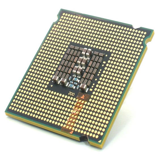
Questo è il substrato del pacchetto FC BGA. Possiamo anche utilizzare questa tecnologia FCBGA per produrre schede madri di fascia alta. ma per favore non progettare unità di dimensioni troppo grandi. se il passo della palla è compreso tra 160um e 250um. è necessario progettare le dimensioni dell'unità in 55 mm*55 mm. se il passo della palla è più grande di 250um 350. puoi progettare le dimensioni della scheda madre in 100 mm * 100 mm.
Se hai domande, non esitate a contattarci coninfo@alcantapcb.com , Saremo felici di aiutarti.