CO.,LTD")
Produttore di substrati per array di griglie a sfere Flip Chip. Come leader Flip Chip Produttore di substrati per array di griglie a sfere, siamo specializzati nella produzione di substrati ad alte prestazioni per applicazioni elettroniche avanzate. I nostri processi produttivi all’avanguardia garantiscono qualità e affidabilità superiori, soddisfare le esigenze di settori come quello delle telecomunicazioni, informatica, e automobilistico. Sfruttando tecnologia all’avanguardia e design innovativo, forniamo soluzioni che migliorano le prestazioni del dispositivo, supportare la miniaturizzazione, e garantire una solida integrità termica e del segnale.
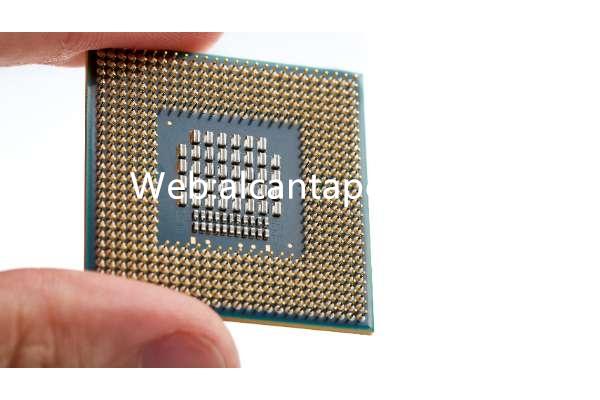
La matrice della griglia di sfere Flip Chip (FC-BGA) substrato è un componente critico nel moderno imballaggio elettronico, offrendo una soluzione robusta per applicazioni ad alte prestazioni e ad alta densità. I substrati FC-BGA sono progettati per supportare chip semiconduttori avanzati, fornire collegamenti elettrici, supporto meccanico, e dissipazione del calore. Questi substrati svolgono un ruolo fondamentale nel migliorare le prestazioni e l'affidabilità dei circuiti integrati (circuiti integrati) in varie applicazioni, spaziando dall'elettronica di consumo ai sistemi automobilistici. In questo articolo, approfondiremo le complessità dei substrati FC-BGA, esplorandone la struttura, materiali, processi di produzione, aree di applicazione, e vantaggi.
Cos'è un substrato FC-BGA?
Un substrato FC-BGA è un tipo di tecnologia di confezionamento utilizzata per montare chip semiconduttori direttamente su un substrato con protuberanze di saldatura. A differenza del tradizionale wire bonding, la tecnologia flip chip capovolge il chip, consentendo all'area attiva di essere rivolta verso il substrato. Questo metodo offre diversi vantaggi, comprese le interconnessioni a densità più elevata, miglioramento delle prestazioni elettriche, e una migliore gestione termica.
Il substrato FC-BGA è costituito da più strati, compreso uno strato centrale, strati di accumulo, e strati di maschera di saldatura. Lo strato centrale è tipicamente costituito da materiali come la bismaleimide-triazina (BT) resina o resina epossidica, che offrono ottima stabilità termica e resistenza meccanica. Strati di costruzione, realizzato con materiali dielettrici e rame, vengono aggiunti per creare l'intricato cablaggio richiesto per le interconnessioni ad alta densità. Gli strati della maschera di saldatura proteggono i circuiti e impediscono i ponti di saldatura durante l'assemblaggio.
Le interconnessioni tra il chip e il substrato vengono formate utilizzando protuberanze di saldatura, che sono piccole sfere di materiale di saldatura posizionate sui pad I/O del chip. Durante il montaggio, il chip viene capovolto e allineato con il substrato, e i rilievi di saldatura vengono rifusi per creare una robusta connessione meccanica ed elettrica. Questo processo consente un numero maggiore di interconnessioni per unità di area rispetto al tradizionale wire bonding.
Struttura dei substrati FC-BGA
La struttura dei substrati FC-BGA è complessa e altamente ingegnerizzata per soddisfare le esigenze del packaging avanzato dei semiconduttori. I substrati sono generalmente costituiti da diversi componenti chiave:
Lo strato centrale fornisce la struttura meccanica del substrato. Materiali come la resina BT o la resina epossidica sono comunemente utilizzati grazie alle loro eccellenti proprietà termiche e meccaniche. Lo strato centrale è tipicamente rigido, offrendo stabilità e supporto all'intera struttura del substrato.
Vengono aggiunti più strati di accumulo su entrambi i lati dello strato centrale per creare il percorso necessario per i segnali elettrici. Questi strati sono costituiti da materiali dielettrici, come il rame rivestito di resina (RCC) o epossidico, e sono intervallati da tracce di rame. Gli strati di costruzione consentono il cablaggio ad alta densità richiesto per i circuiti integrati avanzati, consentendo instradamenti complessi e molteplici livelli di interconnessioni.
Gli strati della maschera di saldatura vengono applicati sopra gli strati di accumulo per proteggere i circuiti e prevenire i ponti di saldatura. Questi strati sono realizzati con materiali isolanti e sono fondamentali per mantenere l'integrità dei collegamenti elettrici durante l'assemblaggio e il funzionamento.
I dossi di saldatura sono piccole sfere di materiale di saldatura posizionate sui pad I/O del chip. Questi dossi creano la connessione elettrica e meccanica tra il chip e il substrato. I rilievi di saldatura sono generalmente realizzati con materiali di saldatura senza piombo, come stagno-argento-rame (SAC) leghe, per rispettare le normative ambientali.
La struttura complessiva di un substrato FC-BGA è progettata per ottimizzare le prestazioni elettriche, gestione termica, e stabilità meccanica. La combinazione degli strati centrali, strati di accumulo, strati della maschera di saldatura, e le protuberanze di saldatura garantiscono un funzionamento affidabile in applicazioni impegnative.
Materiali utilizzati nei substrati FC-BGA
I materiali utilizzati nei substrati FC-BGA sono accuratamente selezionati per soddisfare i severi requisiti del packaging dei semiconduttori ad alte prestazioni. I materiali chiave includono:
Lo strato centrale è generalmente costituito da resina BT o resina epossidica. La resina BT è apprezzata per la sua eccellente stabilità termica, costante dielettrica bassa, e buona resistenza meccanica. I materiali epossidici vengono utilizzati anche per la loro convenienza e prestazioni adeguate in molte applicazioni.
Gli strati di costruzione utilizzano materiali dielettrici come RCC o resina epossidica per isolare le tracce di rame e garantire l'integrità strutturale. I materiali RCC sono noti per la loro bassa dilatazione termica e l'elevata affidabilità, rendendoli adatti per interconnessioni ad alta densità.
Il rame è ampiamente utilizzato per le tracce conduttive negli strati di costruzione. Offre un'eccellente conduttività elettrica, conduttività termica, e affidabilità. Gli strati di rame sono tipicamente formati attraverso processi di galvanica, consentendo un controllo preciso delle dimensioni e dello spessore della traccia.
Gli strati della maschera di saldatura sono realizzati con materiali isolanti che proteggono i circuiti sottostanti e impediscono i ponti di saldatura. Questi materiali sono tipicamente a base epossidica e vengono applicati utilizzando tecniche di serigrafia o di imaging fotografico.
I dossi di saldatura sono realizzati con materiali di saldatura senza piombo, come le leghe SAC. Questi materiali offrono buone proprietà meccaniche, ottima resistenza alla fatica termica, e il rispetto delle normative ambientali.
L'attenta selezione e combinazione di questi materiali sono cruciali per ottenere l'effetto elettrico desiderato, termico, e prestazioni meccaniche dei substrati FC-BGA. Ciascun materiale contribuisce all'affidabilità e alle prestazioni complessive del substrato, garantendo che soddisfi le esigenze del packaging avanzato dei semiconduttori.
Til processo di produzione dei substrati FC-BGA
Il processo di produzione dei substrati FC-BGA prevede diverse fasi complesse, ciascuno contribuisce alla qualità complessiva e alle prestazioni del prodotto finale. Il processo include:
Il primo passo prevede la preparazione dei materiali di base, materiali dielettrici, e lamine di rame. I materiali del nucleo sono tipicamente laminati con fogli di rame per formare il substrato iniziale.
Per substrati multistrato, più strati di dielettrico e rame vengono impilati e legati insieme utilizzando processi di laminazione. Questo passaggio richiede un allineamento e un controllo precisi per garantire la corretta registrazione e l'incollaggio di ogni strato.
Dopo l'impilamento degli strati, i fori vengono praticati nel substrato per creare vie e fori passanti. Tecniche di perforazione avanzate, come la perforazione laser, può essere utilizzato per microvie e requisiti di alta precisione. I fori praticati vengono quindi puliti e preparati per la placcatura.
I fori praticati sono placcati in rame per creare collegamenti elettrici tra gli strati. Si tratta del deposito di un sottile strato di rame sulle pareti dei fori attraverso processi di galvanica. Il processo di placcatura deve essere attentamente controllato per garantire copertura e adesione uniformi.
Gli schemi circuitali desiderati vengono trasferiti sugli strati di rame mediante un processo fotolitografico. Ciò comporta l'applicazione di una pellicola fotosensibile (fotoresist) alla superficie di rame ed esponendolo ai raggi ultravioletti (UV) luce attraverso una fotomaschera. Le aree esposte del fotoresist vengono sviluppate, lasciando dietro di sé lo schema del circuito. La scheda viene quindi incisa per rimuovere il rame indesiderato, lasciando solo le tracce del circuito.
Alla scheda viene applicata una maschera di saldatura per proteggere i circuiti ed evitare ponti di saldatura. La maschera di saldatura viene generalmente applicata utilizzando tecniche di serigrafia o di imaging fotografico e quindi polimerizzata per indurirla.
Una finitura superficiale viene applicata alle aree di rame esposte per migliorare la saldabilità e proteggere dall'ossidazione. Le finiture superficiali comuni includono l'oro ad immersione in nichel chimico (ESSERE D'ACCORDO), Livellamento della saldatura ad aria calda (HASL), e Argento Immersione.
I rilievi di saldatura sono posizionati sui pad I/O del chip, e il chip viene quindi capovolto e allineato con il substrato. I rilievi di saldatura vengono rifusi per creare una robusta connessione meccanica ed elettrica tra il chip e il substrato.
La fase finale prevede test e ispezioni rigorosi per garantire che il substrato soddisfi tutti i requisiti di prestazioni e affidabilità. Test elettrici, ispezione visiva, e ispezione ottica automatizzata (AOI) servono per individuare eventuali difetti o irregolarità. Eventuali problemi identificati durante i test vengono risolti prima che i substrati vengano approvati per la spedizione.
Il processo di produzione dei substrati FC-BGA richiede controllo preciso e competenza per garantire alta qualità e affidabilità. Ogni passaggio è fondamentale per ottenere le prestazioni e l'affidabilità desiderate del prodotto finale.
Aree di applicazione dei substrati FC-BGA
I substrati FC-BGA sono utilizzati in un'ampia gamma di applicazioni in vari settori grazie alle loro elevate prestazioni e affidabilità. Le principali aree di applicazione includono:
I substrati FC-BGA sono ampiamente utilizzati nell'elettronica di consumo, come gli smartphone, compresse, e console di gioco. Questi dispositivi richiedono circuiti integrati ad alte prestazioni con soluzioni di packaging avanzate per ottenere le prestazioni e il fattore di forma desiderati. I substrati FC-BGA forniscono le interconnessioni necessarie, gestione termica, e supporto meccanico per questi chip ad alte prestazioni.
L'industria automobilistica fa affidamento sull'elettronica avanzata per varie applicazioni, comprese le centraline motore (ECU), sistemi avanzati di assistenza alla guida (ADAS), e sistemi di infotainment. I substrati FC-BGA offrono un'elevata affidabilità, gestione termica, e la stabilità meccanica richiesta per le applicazioni automobilistiche, garantire il funzionamento sicuro ed efficiente dei sistemi elettronici nei veicoli.
Nelle telecomunicazioni, I substrati FC-BGA vengono utilizzati nelle stazioni base, infrastruttura di rete, e dispositivi di comunicazione. Le interconnessioni ad alta densità e le prestazioni elettriche superiori dei substrati FC-BGA li rendono ideali per gestire i segnali ad alta frequenza e le velocità dati richieste nei moderni sistemi di comunicazione.
Dispositivi medici, come i sistemi di imaging, apparecchiature diagnostiche, e dispositivi di monitoraggio dei pazienti, richiedono circuiti integrati affidabili e ad alte prestazioni. I substrati FC-BGA forniscono le prestazioni elettriche necessarie, gestione termica, e affidabilità per queste applicazioni critiche, garantire il funzionamento accurato e coerente dei dispositivi medici.
Nell'elettronica industriale, I substrati FC-BGA sono utilizzati nei sistemi di automazione, gestione dell'energia, e sistemi di controllo. Queste applicazioni richiedono soluzioni di imballaggio robuste e affidabili per resistere a condizioni ambientali difficili e garantire un funzionamento continuo. I substrati FC-BGA offrono le prestazioni e la durata necessarie per le applicazioni industriali.
Le applicazioni aerospaziali e di difesa richiedono sistemi elettronici ad alta affidabilità e ad alte prestazioni. I substrati FC-BGA sono utilizzati nei sistemi radar, apparecchiature di comunicazione, e avionica, fornendo le prestazioni elettriche necessarie, gestione termica, e stabilità meccanica per applicazioni mission-critical.
Vantaggi dei substrati FC-BGA
I substrati FC-BGA offrono numerosi vantaggi che li rendono la scelta preferita per applicazioni ad alte prestazioni e alta affidabilità. Questi vantaggi includono:
I substrati FC-BGA consentono un numero elevato di interconnessioni per unità di area, consentendo progetti di circuiti integrati più complessi e ad alte prestazioni. Questa elevata densità è ottenuta attraverso l'uso di protuberanze di saldatura e strutture multistrato avanzate, fornendo prestazioni elettriche e integrità del segnale superiori.
La tecnologia flip chip utilizzata nei substrati FC-BGA offre percorsi del segnale più brevi e diretti rispetto al tradizionale wire bonding. Ciò si traduce in una minore perdita di segnale, ridotta induttanza e capacità parassita, e una migliore integrità del segnale, rendendo i substrati FC-BGA ideali per applicazioni ad alta frequenza e ad alta velocità.
I substrati FC-BGA forniscono una gestione termica efficiente attraverso l'uso di materiali con elevata conduttività termica e strutture ottimizzate. La configurazione del chip flip consente inoltre la dissipazione diretta del calore dal chip al substrato, riducendo la resistenza termica e migliorando la dissipazione del calore. Ciò è fondamentale per le applicazioni ad alta potenza in cui un'efficace gestione termica è essenziale per un funzionamento affidabile.
La struttura robusta dei substrati FC-BGA, compreso l'uso di resina BT o materiali epossidici, fornisce eccellente stabilità meccanica e affidabilità. Ciò garantisce che i substrati possano resistere alle sollecitazioni meccaniche, Ciclismo termico, e condizioni ambientali difficili senza compromettere le prestazioni.
I substrati FC-BGA offrono scalabilità in termini sia di prestazioni che di produzione. La tecnologia consente l'integrazione di più chip e funzioni su un unico substrato, consentendo lo sviluppo di sistemi avanzati nel pacchetto (Sorso) soluzioni. Inoltre, i processi di produzione dei substrati FC-BGA sono compatibili con la produzione in grandi volumi, rendendoli adatti sia per l'elettronica di consumo a basso costo che per le applicazioni industriali di fascia alta.
I substrati FC-BGA sono versatili e possono essere utilizzati in un'ampia gamma di applicazioni, dall'elettronica di consumo all'automotive, telecomunicazioni, dispositivi medici, elettronica industriale, e aerospaziale e difesa. La combinazione di alte prestazioni, affidabilità, e la scalabilità rendono i substrati FC-BGA la scelta ideale per vari settori e applicazioni.
Domande frequenti
Ciò che rende i substrati FC-BGA diversi dai substrati BGA tradizionali?
I substrati FC-BGA differiscono dai substrati BGA tradizionali principalmente per l'uso della tecnologia flip chip. Nei substrati FC-BGA, il chip viene capovolto e collegato al substrato mediante protuberanze di saldatura, con conseguente interconnessione a densità più elevata, miglioramento delle prestazioni elettriche, e una migliore gestione termica. I substrati BGA tradizionali utilizzano il wire bonding, che potrebbero non offrire lo stesso livello di prestazioni in applicazioni ad alta frequenza e ad alta potenza.
I substrati FC-BGA possono essere utilizzati in applicazioni ad alta potenza?
SÌ, I substrati FC-BGA sono particolarmente adatti per applicazioni ad alta potenza. La configurazione del flip chip consente la dissipazione diretta del calore dal chip al substrato, riducendo la resistenza termica e migliorando la gestione termica. Ciò rende i substrati FC-BGA ideali per applicazioni come gli amplificatori di potenza, Elettronica automobilistica, e sistemi industriali in cui un'efficace dissipazione del calore è fondamentale per un funzionamento affidabile.
I substrati FC-BGA sono adatti all'uso in ambienti difficili?
I substrati FC-BGA sono particolarmente adatti per l'uso in ambienti difficili. La struttura robusta, compreso l'uso di materiali con eccellenti proprietà termiche e meccaniche, garantisce prestazioni affidabili in condizioni ambientali variabili, come le alte temperature, umidità, e stress meccanico. Ciò rende i substrati FC-BGA una scelta eccellente per il settore automobilistico, aerospaziale, e applicazioni di difesa in cui l'affidabilità in condizioni estreme è fondamentale.
In che modo il processo di produzione dei substrati FC-BGA garantisce alta qualità e affidabilità?
Il processo di produzione dei substrati FC-BGA prevede diverse fasi complesse, compresa la preparazione del materiale, impilamento degli strati, perforazione, placcatura, immagine, acquaforte, applicazione della maschera di saldatura, finitura superficiale, posizionamento della protuberanza della saldatura, e test e ispezioni rigorosi. Ogni passaggio è attentamente controllato e monitorato per garantire alta qualità e affidabilità. Tecniche avanzate come la perforazione laser, galvanica, e ispezione ottica automatizzata (AOI) vengono utilizzati per ottenere risultati precisi e coerenti. Questo meticoloso processo garantisce che i substrati FC-BGA soddisfino i rigorosi requisiti di prestazioni e affidabilità degli imballaggi per semiconduttori ad alte prestazioni.