CO.,LTD")
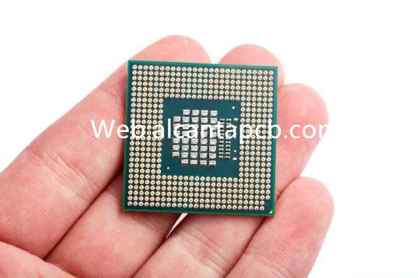
FCCSP (Pacchetto bilancia Flip Chip Chip) produttore di substrati, FCCSP ultra multistrato (Flip Chip Pacchetto scala chip) I substrati sono soluzioni di packaging avanzate progettate per supportare la crescente complessità e le richieste di prestazioni dei moderni dispositivi elettronici. Questi substrati presentano più strati di circuiti, consentendo interconnessioni ad alta densità e una gestione termica efficiente. I substrati FCCSP ultra multistrato sono cruciali nelle applicazioni in cui la miniaturizzazione, alte prestazioni, e l'affidabilità sono essenziali, come negli smartphone, calcolo ad alte prestazioni, e telecomunicazioni.
Cos'è un substrato FCCSP ultra multistrato?
Un substrato FCCSP ultra-multistrato è un tipo di substrato del pacchetto semiconduttore progettato per supportare il collegamento di flip chip e più strati di circuiti. La tecnologia FCCSP prevede il montaggio del dischetto del semiconduttore a faccia in giù sul substrato, consentendo connessioni elettriche dirette tra lo stampo e il substrato tramite protuberanze di saldatura. Questo metodo di confezionamento riduce le dimensioni del pacco e migliora le prestazioni elettriche minimizzando la lunghezza delle interconnessioni.
IL “ultra multistrato” L'aspetto si riferisce all'uso di più strati di circuiti all'interno del substrato. Questi strati consentono il routing ad alta densità di segnali e potenza, che è essenziale per supportare il funzionamento complesso e ad alta velocità dei moderni dispositivi a semiconduttore. I substrati FCCSP ultra multistrato forniscono una migliore integrità del segnale, efficiente distribuzione dell’energia, e una migliore gestione termica, rendendoli ideali per applicazioni ad alte prestazioni.
Guida di riferimento alla progettazione del substrato FCCSP ultra multistrato
La progettazione di substrati FCCSP ultra-multistrato implica diverse considerazioni critiche per garantire prestazioni e affidabilità ottimali. Le sezioni seguenti forniscono una panoramica degli aspetti chiave coinvolti nella progettazione e nell'applicazione di questi substrati.
I materiali utilizzati nei substrati FCCSP ultra-multistrato sono selezionati per le loro proprietà elettriche superiori, termico, e proprietà meccaniche:
Materiali dielettrici ad alte prestazioni: Materiali dielettrici avanzati, come poliimmidi e polimeri a cristalli liquidi, sono utilizzati per fornire un eccellente isolamento elettrico e supportare la trasmissione del segnale ad alta frequenza.
Rame: Per le tracce conduttive vengono utilizzati strati di rame ultrasottili, offrendo un'eccellente conduttività elettrica e consentendo la modellazione a linee sottili necessaria per le interconnessioni ad alta densità.
Maschera per saldatura: Viene applicata una maschera di saldatura ad alta precisione per proteggere i circuiti sottostanti ed evitare ponti di saldatura durante l'assemblaggio. La maschera di saldatura deve resistere alle alte temperature della saldatura a rifusione e di altri processi di assemblaggio.
Adesivi: Per unire insieme gli strati vengono utilizzati adesivi avanzati, garantendo stabilità meccanica e minimizzando la perdita di segnale.
Durante la fase di progettazione è necessario affrontare diverse considerazioni chiave:
Controllo dell'impedenza: Il controllo preciso dell'impedenza è essenziale per mantenere l'integrità del segnale, soprattutto alle alte frequenze. Ciò comporta un'attenta progettazione delle tracce del segnale e l'uso di materiali ad impedenza controllata.
Gestione termica: Una gestione termica efficace è fondamentale per le applicazioni ad alte prestazioni. Il progetto deve incorporare vie termiche, dissipatori di calore, o altre tecniche per dissipare in modo efficiente il calore generato da componenti ad alta potenza.
Stabilità meccanica: Il substrato deve fornire un supporto meccanico robusto per resistere ai cicli termici e alle sollecitazioni meccaniche durante il funzionamento.
Affidabilità: L'affidabilità a lungo termine è garantita dall'uso di materiali di alta qualità e processi di produzione precisi, prevenendo problemi come la delaminazione e la deformazione.
Quali materiali vengono utilizzati nei substrati FCCSP ultra multistrato?
I materiali utilizzati nei substrati FCCSP ultra-multistrato sono selezionati per le loro proprietà complementari volte a migliorare le prestazioni complessive del substrato:
Materiali dielettrici ad alte prestazioni: I materiali dielettrici avanzati forniscono isolamento elettrico e supportano la trasmissione del segnale ad alta frequenza.
Rame: Per gli strati conduttivi viene utilizzato rame di elevata purezza, offrendo un'eccellente conduttività elettrica e consentendo la modellazione di linee sottili.
Maschera per saldatura: Un sottile, la maschera di saldatura ad alta precisione protegge i circuiti sottostanti e previene i ponti di saldatura durante l'assemblaggio, resistere alle alte temperature della saldatura a rifusione.
Adesivi avanzati: Adesivi specializzati uniscono insieme gli strati, fornendo stabilità meccanica e minimizzando la perdita di segnale.
Di quali dimensioni sono i substrati FCCSP ultra multistrato?
La dimensione dei substrati FCCSP Ultra-Multistrato varia a seconda dell'applicazione e dei requisiti di progettazione specifici:
Spessore: Lo spessore complessivo dei substrati FCCSP ultra multistrato può variare da poche centinaia di micrometri a oltre un millimetro, a seconda del numero di strati e dei requisiti applicativi.
Dimensioni: La lunghezza e la larghezza dei substrati sono determinate dalla dimensione dei componenti e dalla disposizione del sistema. Possono variare da piccoli fattori di forma per dispositivi compatti a substrati più grandi per sistemi elettronici più complessi.
Il processo di produzione dei substrati FCCSP ultra-multistrato
Il processo di produzione dei substrati FCCSP Ultra-Multistrato prevede diverse fasi precise e controllate per garantire qualità e prestazioni elevate:
Materiali di base di alta qualità, come laminati rivestiti in rame e materiali dielettrici avanzati, vengono selezionati e preparati per la lavorazione. I materiali vengono puliti e trattati per rimuovere eventuali impurità e garantire una superficie liscia.
Il materiale dielettrico viene applicato al substrato in più strati, con ciascuno strato che viene modellato e polimerizzato per formare i modelli di circuito desiderati. Questo processo viene ripetuto per creare il numero richiesto di strati, garantendo interconnessioni ad alta densità e prestazioni elettriche eccellenti.
Microvie e fori passanti vengono praticati nel substrato per creare connessioni elettriche tra gli strati. Questi passaggi vengono quindi placcati in rame per garantire una conduttività elettrica affidabile e un robusto supporto meccanico.
La superficie del substrato è rifinita con una maschera di saldatura ad alta precisione per proteggere i circuiti sottostanti e fornire una superficie liscia per il montaggio dei componenti. Questa fase prevede anche l'applicazione delle finiture superficiali, come ENIG (Oro per immersione in nichel chimico) o OSP (Conservante organico di saldabilità), per migliorare la saldabilità e la resistenza alla corrosione.
Dopo la fabbricazione, i substrati sono assemblati con componenti elettronici. Vengono condotti test rigorosi per garantire che i substrati soddisfino tutte le specifiche di progettazione e i requisiti prestazionali. Ciò include test elettrici, Ciclismo termico, e prove di stress meccanico per verificare l'affidabilità e la durabilità dei substrati.
L'area di applicazione dei substrati FCCSP ultra-multistrato
I substrati FCCSP ultra multistrato sono utilizzati in un'ampia gamma di applicazioni elettroniche ad alte prestazioni:
Nell'elettronica di consumo, I substrati FCCSP ultra multistrato supportano dispositivi compatti e ad alte prestazioni come gli smartphone, compresse, e tecnologia indossabile. I substrati forniscono le prestazioni elettriche e termiche necessarie per garantire il funzionamento affidabile di questi dispositivi.
Nei dispositivi medici, I substrati FCCSP ultra multistrato supportano l'elaborazione del segnale ad alta frequenza e il funzionamento affidabile in varie apparecchiature diagnostiche e terapeutiche. Questi substrati garantiscono una trasmissione del segnale precisa e accurata, rendendoli ideali per l'uso nei sistemi di imaging, dispositivi di monitoraggio, e strumenti chirurgici.
Nelle applicazioni automobilistiche, I substrati FCCSP ultra multistrato sono utilizzati in vari sistemi elettronici, compreso l'infotainment, navigazione, e sistemi avanzati di assistenza alla guida (ADAS). Questi substrati offrono affidabilità e prestazioni elevate, consentendo funzionalità avanzate e funzionamento efficiente negli ambienti automobilistici.
Nelle applicazioni aerospaziali e della difesa, I substrati FCCSP ultra multistrato forniscono prestazioni robuste in ambienti difficili e in condizioni estreme. Questi substrati sono utilizzati in vari sistemi aerospaziali e di difesa, come il radar, comunicazione, e sistemi di navigazione, garantendo un funzionamento affidabile e una durata a lungo termine.
Nell'automazione industriale, I substrati FCCSP ultra multistrato sono utilizzati in vari sistemi di controllo e automazione. Questi substrati offrono affidabilità e prestazioni elevate, consentendo funzionalità avanzate e funzionamento efficiente in ambienti industriali.
Quali sono i vantaggi dei substrati FCCSP ultra multistrato?
I substrati FCCSP ultra multistrato offrono numerosi vantaggi che li rendono indispensabili nelle applicazioni elettroniche ad alte prestazioni:
Alte prestazioni: I substrati FCCSP ultra multistrato forniscono un'elaborazione del segnale ad alta velocità e un'eccellente integrità del segnale, rendendoli ideali per dispositivi e sistemi elettronici avanzati.
Miniaturizzazione: Questi substrati consentono l'integrazione di circuiti complessi in un fattore di forma compatto, sostenere la tendenza verso dispositivi elettronici più piccoli e più potenti.
Gestione termica: Questi substrati offrono una migliore gestione termica, dissipare in modo efficiente il calore generato da componenti ad alta potenza e garantire un funzionamento affidabile.
Deformazione ridotta: L'uso di materiali avanzati e processi di produzione precisi riduce il rischio di deformazioni, migliorando la stabilità meccanica e l’affidabilità del substrato.
Affidabilità: I substrati FCCSP ultra multistrato forniscono un robusto supporto meccanico, Efficiente gestione termica, e affidabilità a lungo termine, garantire il funzionamento stabile dei dispositivi elettronici.
Versatilità: I substrati FCCSP ultra multistrato possono essere utilizzati in un'ampia gamma di applicazioni, dall'elettronica di consumo e dai dispositivi medici all'automotive e all'aerospaziale, fornendo funzionalità avanzate e affidabilità in ambienti esigenti.
Domande frequenti
Quali sono le considerazioni chiave nella progettazione di un substrato FCCSP ultra multistrato?
Le considerazioni chiave includono le proprietà dei materiali, impilamento degli strati, controllo dell'impedenza, gestione termica, e stabilità meccanica. Il design dovrebbe garantire prestazioni elettriche ottimali, efficiente dissipazione del calore, e affidabilità a lungo termine.
In che modo i substrati FCCSP ultra-multistrato differiscono dai substrati FCCSP tradizionali?
I substrati FCCSP ultra multistrato presentano più strati di circuiti, consentendo instradamento ad alta densità e prestazioni elettriche migliorate rispetto ai tradizionali substrati FCCSP, che può avere meno strati e interconnessioni a densità inferiore.
Qual è il tipico processo di produzione dei substrati FCCSP ultra multistrato?
Il processo prevede la preparazione del materiale, accumulo di strati, foratura e placcatura, finitura superficiale, e assemblaggio e collaudo. Ogni passaggio è attentamente controllato per garantire alta qualità e prestazioni.