株式会社")
fccsp (フリップチップチップスケールパッケージ) substrates manufacturer, 超多層 FCCSP (フリップチップ チップスケールパッケージ) substrates are advanced packaging solutions designed to support the increasing complexity and performance demands of modern electronic devices. These substrates feature multiple layers of circuitry, enabling high-density interconnects and efficient thermal management. Ultra-Multilayer FCCSP substrates are crucial in applications where miniaturization, 高性能, と信頼性が不可欠です, スマートフォンなどの, ハイパフォーマンスコンピューティング, と電気通信.
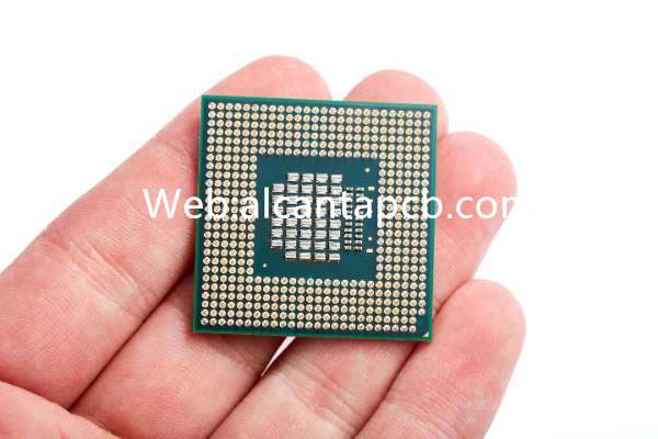
What is an Ultra-Multilayer FCCSP Substrate?
An Ultra-Multilayer FCCSP substrate is a type of semiconductor package substrate designed to support flip chip bonding and multiple layers of circuitry. The FCCSP technology involves mounting the semiconductor die face-down on the substrate, allowing for direct electrical connections between the die and the substrate via solder bumps. This packaging method reduces the package size and enhances electrical performance by minimizing the length of the interconnections.
の “超多層” aspect refers to the use of multiple layers of circuitry within the substrate. These layers enable high-density routing of signals and power, which is essential for supporting the complex and high-speed operation of modern semiconductor devices. Ultra-Multilayer FCCSP substrates provide improved signal integrity, 効率的な電力分配, 強化された熱管理, 高性能アプリケーションに最適です.
Ultra-Multilayer FCCSP Substrate Design Reference Guide
Designing Ultra-Multilayer FCCSP substrates involves several critical considerations to ensure optimal performance and reliability. 次のセクションでは、これらの基質の設計と適用に関連する重要な側面の概要を示します。.
The materials used in Ultra-Multilayer FCCSP substrates are selected for their superior electrical, 熱, および機械的特性:
高性能誘電体材料: Advanced dielectric materials, such as polyimides and liquid crystal polymers, are used to provide excellent electrical insulation and support high-frequency signal transmission.
銅: 導電性トレースには極薄の銅層が使用されています, offering excellent electrical conductivity and allowing for fine-line patterning necessary for high-density interconnects.
はんだマスク: A high-precision solder mask is applied to protect the underlying circuitry and prevent solder bridging during assembly. The solder mask must withstand the high temperatures of reflow soldering and other assembly processes.
Adhesives: 高度な接着剤は、層を結合するために使用されます, 機械的安定性を確保し、信号損失を最小限に抑えます.
設計段階では、いくつかの重要な考慮事項に対処する必要があります:
インピーダンス制御: 信号の完全性を維持するには、正確なインピーダンス制御が不可欠です, 特に高周波では. これには、信号トレースの慎重な設計と、制御されたインピーダンス材料の使用が含まれます。.
熱管理: 高性能アプリケーションには効果的な熱管理が不可欠です. 設計にはサーマルビアを組み込む必要があります, ヒートシンク, 高出力コンポーネントによって生成される熱を効率的に放散するためのその他の技術.
機械的安定性: 基板は、動作中の熱サイクルや機械的ストレスに耐えられるように、堅牢な機械的サポートを提供する必要があります。.
信頼性: 高品質の材料と精密な製造プロセスの使用により長期信頼性が保証されます。, 剥離や反りなどの問題を防止.
What Materials are Used in Ultra-Multilayer FCCSP Substrates?
Materials used in Ultra-Multilayer FCCSP substrates are selected for their complementary properties to enhance the overall performance of the substrate:
高性能誘電体材料: Advanced dielectric materials provide electrical insulation and support high-frequency signal transmission.
銅: High-purity copper is used for the conductive layers, offering excellent electrical conductivity and enabling fine-line patterning.
はんだマスク: 薄い, 高精度のはんだマスクが下層の回路を保護し、組み立て中のはんだブリッジを防止します。, リフローはんだ付けの高温に耐える.
高度な接着剤: 特殊な接着剤が層を接着します, 機械的な安定性を提供し、信号損失を最小限に抑えます。.
What Size are Ultra-Multilayer FCCSP Substrates?
The size of Ultra-Multilayer FCCSP substrates varies depending on the application and specific design requirements:
厚さ: The overall thickness of Ultra-Multilayer FCCSP substrates can range from a few hundred micrometers to over a millimeter, レイヤーの数とアプリケーション要件に応じて.
寸法: 基板の長さと幅は、コンポーネントのサイズとシステムのレイアウトによって決まります。. 小型デバイス用の小さなフォームファクタから、より複雑な電子システム用の大型基板まで多岐にわたります。.
The Manufacturing Process of Ultra-Multilayer FCCSP Substrates
The manufacturing process of Ultra-Multilayer FCCSP substrates involves several precise and controlled steps to ensure high quality and performance:
高品質のベース材料, such as copper-clad laminates and advanced dielectric materials, 処理のために選択され、準備されています. 材料は、不純物を除去し、滑らかな表面を確保するために洗浄および処理されます.
誘電体材料は基板に複数の層で塗布されます, 各レイヤーがパターン化され、硬化して、目的の回路パターンを形成するために. このプロセスは、必要なレイヤー数を構築するために繰り返されます, 高密度の相互接続と優れた電気性能を確保します.
マイクロバイアとスルーホールが基板にドリルされ、レイヤー間に電気接続が作成されます. これらのバイアスは、信頼できる電気導電率と堅牢な機械的サポートを確保するために銅でメッキされます.
基板の表面は高精度のはんだマスクで仕上げられており、下にある回路を保護し、コンポーネントの実装に滑らかな表面を提供します。. このステップには、表面仕上げの適用も含まれます, エニグなど (無電解ニッケル浸漬金) またはOSP (有機はんだ付け性保存剤), はんだき性と耐食性を高めるため.
製造後, 基板には電子部品が組み込まれています. 厳密なテストが実施され、基板がすべての設計仕様とパフォーマンス要件を満たしていることを確認します. これには、電気テストが含まれます, 熱サイクル, 基板の信頼性と耐久性を検証するための機械的ストレステスト.
The Application Area of Ultra-Multilayer FCCSP Substrates
Ultra-Multilayer FCCSP substrates are used in a wide range of high-performance electronic applications:
家庭用電化製品において, Ultra-Multilayer FCCSP substrates support high-performance and compact devices such as smartphones, 錠剤, およびウェアラブルテクノロジー. 基板は、これらのデバイスの信頼性の高い動作を保証するために必要な電気的および熱的性能を提供します。.
医療機器において, Ultra-Multilayer FCCSP substrates support high-frequency signal processing and reliable operation in various diagnostic and therapeutic equipment. これらの基板により、正確かつ正確な信号伝送が保証されます。, 画像処理システムでの使用に最適です, 監視装置, および手術器具.
自動車用途において, Ultra-Multilayer FCCSP substrates are used in various electronic systems, インフォテイメントを含む, ナビゲーション, および先進運転支援システム (ADAS). これらの基板は高い信頼性とパフォーマンスを提供します, 自動車環境における高度な機能と効率的な運用を可能にする.
航空宇宙および防衛用途, Ultra-Multilayer FCCSP substrates provide robust performance in harsh environments and under extreme conditions. これらの基板はさまざまな航空宇宙および防衛システムで使用されています, レーダーなどの, コミュニケーション, およびナビゲーションシステム, 信頼できる操作と長期的な耐久性を確保します.
産業オートメーションにおいて, Ultra-Multilayer FCCSP substrates are used in various control and automation systems. これらの基板は高い信頼性とパフォーマンスを提供します, 産業環境での高度な機能と効率的な運用を可能にします.
What are the Advantages of Ultra-Multilayer FCCSP Substrates?
Ultra-Multilayer FCCSP substrates offer several advantages that make them indispensable in high-performance electronic applications:
高性能: Ultra-Multilayer FCCSP substrates provide high-speed signal processing and excellent signal integrity, 先進的な電子機器やシステムに最適です。.
小型化: これらの基板により、複雑な回路をコンパクトなフォームファクターに統合できます。, 電子機器の小型化と高性能化の傾向をサポート.
熱管理: これらの基板は強化された熱管理を提供します, 高出力コンポーネントから発生する熱を効率的に放散し、信頼性の高い動作を保証します。.
Reduced Warpage: The use of advanced materials and precise manufacturing processes reduces the risk of warpage, improving the mechanical stability and reliability of the substrate.
信頼性: Ultra-Multilayer FCCSP substrates provide robust mechanical support, 効率的な熱管理, 長期的な信頼性, 電子機器の安定動作を確保する.
多用途性: Ultra-Multilayer FCCSP substrates can be used in a wide range of applications, 家庭用電化製品や医療機器から自動車や航空宇宙まで, 要求の厳しい環境において高度な機能と信頼性を提供します.
よくある質問
What are the key considerations in designing an Ultra-Multilayer FCCSP substrate?
重要な考慮事項には、材料特性が含まれます, レイヤースタックアップ, インピーダンス制御, 熱管理, 機械的安定性. 設計は、最適な電気性能を確保する必要があります, 効率的な熱放散, 長期的な信頼性.
How do Ultra-Multilayer FCCSP substrates differ from traditional FCCSP substrates?
Ultra-Multilayer FCCSP substrates feature multiple layers of circuitry, enabling high-density routing and enhanced electrical performance compared to traditional FCCSP substrates, which may have fewer layers and lower density interconnects.
What is the typical manufacturing process for Ultra-Multilayer FCCSP substrates?
プロセスには材料の準備が含まれます, 層の構築, 穴あけとメッキ, 表面仕上げ, アセンブリとテスト. 高品質とパフォーマンスを確保するために、各ステップは注意深く管理されています.