CO.,LTD")
Produttore di substrati GPU.”Produttore di substrati GPU” si riferisce ad un'azienda specializzata nella produzione di substrati progettati specificatamente per le unità di elaborazione grafica (GPU). Questi substrati sono componenti cruciali che facilitano interconnessioni elettroniche efficienti e la gestione termica all'interno dei sistemi GPU, garantendo prestazioni e affidabilità ottimali in applicazioni ad alta richiesta come i giochi, intelligenza artificiale, e calcolo scientifico.
I substrati GPU svolgono un ruolo vitale nei moderni dispositivi elettronici, soprattutto nei settori del calcolo ad alte prestazioni e dell'elaborazione grafica. Non solo forniscono supporto fisico per la GPU, migliorano inoltre le prestazioni complessive della GPU attraverso collegamenti elettrici e percorsi termici efficienti. Questo articolo esplorerà in dettaglio la definizione, linee guida di progettazione, materiali, dimensioni, processo di produzione, aree di applicazione, vantaggi, e le domande frequenti sui substrati GPU per aiutare i lettori a comprendere appieno questa tecnologia chiave.
Che cosa sono i substrati GPU?
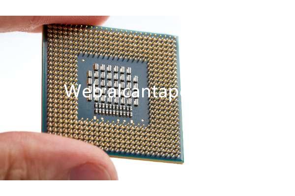
GPU Substrati si riferiscono ai substrati utilizzati per collegare e supportare le unità di elaborazione grafica (GPU) e altri componenti elettronici correlati. La funzione primaria di questi substrati è fornire supporto meccanico, collegamenti elettrici, e percorsi termici per la GPU. Attraverso la sua complessa struttura multistrato, I substrati GPU sono in grado di raggiungere un'interconnessione elettrica ad alta densità in uno spazio limitato garantendo al tempo stesso l'integrità della trasmissione del segnale e la stabilità dell'alimentazione.
Nei moderni dispositivi elettronici, La GPU è il componente principale che consente elaborazione grafica e calcolo ad alte prestazioni. Come la domanda di capacità di elaborazione grafica nei giochi, realtà virtuale, l’intelligenza artificiale e altri campi continuano ad aumentare, Anche i requisiti prestazionali della GPU stanno diventando sempre più elevati. Ciò non solo impone requisiti più elevati al chip GPU stesso, ma impone anche severi standard prestazionali al substrato di imballaggio. Grazie al design multistrato e all'applicazione di materiali altamente conduttivi termicamente, I substrati GPU possono migliorare efficacemente le prestazioni di dissipazione del calore della GPU e garantire che possa ancora funzionare stabilmente con carichi di lavoro ad alto carico.
Inoltre, I substrati GPU devono inoltre soddisfare i requisiti di resistenza meccanica e affidabilità. Poiché le GPU generano grandi quantità di calore e stress meccanico durante il funzionamento, il substrato deve avere resistenza e durabilità sufficienti per prevenire danni strutturali causati dalla dilatazione termica e dalle vibrazioni meccaniche. Ciò richiede che il materiale del substrato non solo abbia un'eccellente conduttività elettrica e termica, ma ha anche buone proprietà meccaniche.
Per realizzare queste funzioni, I substrati GPU utilizzano in genere una combinazione di resine organiche ad alta densità, ceramica, e materiali metallici. Questi materiali formano complesse strutture circuitali multistrato attraverso sofisticati processi di produzione come la laminazione multistrato, galvanica e incisione. Ogni strato di circuiti non viene utilizzato solo per il collegamento elettrico, ma anche per la dissipazione del calore e la schermatura del segnale, garantendo così la stabilità e l'affidabilità della GPU in ambienti di lavoro complessi.
Complessivamente, I substrati GPU svolgono un ruolo vitale nei moderni dispositivi di elaborazione grafica e di elaborazione grafica ad alte prestazioni. Attraverso la progettazione ottimizzata e l'applicazione di materiali avanzati, questi substrati non solo migliorano le prestazioni complessive della GPU, ma promuove anche il continuo progresso della tecnologia di elaborazione grafica.
Guida di riferimento alla progettazione dei substrati GPU
La progettazione di substrati GPU è un compito complesso e delicato che richiede il rispetto di una serie rigorosa di linee guida e standard di progettazione. Primo, la selezione dei materiali è la base del design. I substrati GPU solitamente utilizzano resine organiche ad alta densità (come FR-4), ceramica e materiali metallici. Questi materiali non devono solo avere una buona conduttività elettrica e termica, ma devono anche rimanere stabili in ambienti ad alta temperatura. I materiali ceramici come l'ossido di alluminio e il nitruro di alluminio sono ampiamente utilizzati nelle GPU ad alte prestazioni substrati di imballaggio grazie alla loro elevata conduttività termica e alle eccellenti proprietà di isolamento elettrico.
In secondo luogo, il design della struttura multistrato è il nucleo dei substrati GPU. Il design multistrato consente l'interconnessione elettrica ad alta densità in spazi limitati fornendo allo stesso tempo un efficiente percorso di dissipazione del calore. Il layout del circuito e la progettazione del cablaggio di ogni strato devono essere calcolati e simulati accuratamente per garantire l'integrità della trasmissione del segnale e la stabilità della distribuzione dell'energia. Per l'elaborazione del segnale ad alta frequenza, i progettisti devono prestare particolare attenzione all'adattamento dell'impedenza e alla progettazione della schermatura delle tracce per ridurre la riflessione del segnale e le perdite di radiazioni.
Per garantire l'accuratezza e l'affidabilità dei progetti, i progettisti in genere utilizzano strumenti di progettazione avanzati e software di simulazione. Questi strumenti possono simulare il comportamento dei substrati in diverse condizioni operative, aiutare i progettisti a identificare e risolvere potenziali problemi. Per esempio, un software di simulazione elettromagnetica può simulare la trasmissione di segnali su un substrato e analizzare possibili interferenze e perdite. Il software di simulazione termica può simulare la distribuzione del calore del substrato e aiutare i progettisti a ottimizzare la progettazione della dissipazione del calore.
Inoltre, Anche i test di resistenza meccanica e affidabilità sono aspetti importanti del processo di progettazione. Poiché le GPU generano grandi quantità di calore e stress meccanico durante il funzionamento, il supporto deve avere sufficiente resistenza meccanica e durabilità per evitare danni strutturali causati da dilatazioni termiche e vibrazioni meccaniche. I metodi di prova comuni includono test di resistenza meccanica, prove di ciclo termico e prove di invecchiamento. Questi test possono identificare potenziali problemi con il substrato nell'uso effettivo e garantire che possa funzionare stabilmente in varie condizioni operative.
Finalmente, Il controllo di qualità è fondamentale anche durante il processo di progettazione. Standard e processi di controllo qualità rigorosi garantiscono le prestazioni e l'affidabilità di ciascun substrato. I progettisti devono sviluppare standard e processi dettagliati di controllo della qualità, compresa l'ispezione dei materiali, controllo del processo produttivo, e ispezione del prodotto finito. Attraverso un controllo di qualità completo, il tasso di difetti di produzione può essere notevolmente ridotto e la qualità complessiva del prodotto può essere migliorata.
Per riassumere, la progettazione dei substrati GPU richiede una considerazione completa di molteplici fattori, dalla selezione dei materiali, dalla progettazione strutturale ai test prestazionali e al controllo qualità. Ogni collegamento richiede una progettazione meticolosa e un controllo rigoroso. Seguendo una serie di linee guida e standard di progettazione, i progettisti possono sviluppare substrati di packaging GPU con prestazioni eccellenti ed elevata affidabilità, fornendo una solida base per moderne apparecchiature informatiche e di elaborazione grafica ad alte prestazioni.
Quale materiale viene utilizzato nei substrati GPU?
La selezione dei materiali dei substrati GPU è cruciale. La selezione e l'applicazione di questi materiali influiscono direttamente sulle prestazioni, affidabilità e processo di produzione del substrato. Di seguito sono riportati alcuni materiali comunemente utilizzati e le loro applicazioni e caratteristiche nei substrati GPU.
Prima di tutto, i materiali in resina organica come FR-4 sono i materiali di substrato più comuni. FR-4 è un materiale in resina epossidica rinforzata con fibra di vetro con eccellente resistenza meccanica e proprietà di isolamento elettrico. Non è solo resistente al calore e alla corrosione chimica, ma fornisce anche prestazioni elettriche stabili, quindi è ampiamente utilizzato nella produzione di substrati di vari prodotti elettronici. Per substrati GPU, FR-4 può ridurre ulteriormente lo spessore mantenendo le sue proprietà meccaniche ed elettriche attraverso una formulazione e un processo migliorati.
Anche i materiali ceramici sono una scelta importante nei substrati GPU. I materiali ceramici comunemente usati includono l'ossido di alluminio (Al2O3) e nitruro di alluminio (Aln). Questi materiali hanno proprietà di conduttività termica e di isolamento elettrico estremamente elevate, e può funzionare stabilmente in ambienti ad alta temperatura. L'ossido di alluminio ha buone proprietà meccaniche ed è economico, mentre il nitruro di alluminio è adatto per applicazioni più impegnative grazie alla sua maggiore conduttività termica e proprietà elettriche. Nella progettazione di substrati ultrasottili, i materiali ceramici possono migliorare efficacemente la capacità di dissipazione del calore del substrato e garantire il funzionamento stabile della GPU.
Materiali metallici, come rame e leghe di rame, sono utilizzati principalmente per strati conduttivi e strati di dissipazione del calore nei substrati GPU. Il rame ha un'eccellente conduttività elettrica e termica e può condurre efficacemente segnali elettrici e dissipare il calore. Nella produzione di substrati, I processi di elettroplaccatura e incisione vengono spesso utilizzati per formare modelli conduttivi precisi sul e all'interno del substrato. Per applicazioni ad alte prestazioni, le leghe di rame possono essere utilizzate anche per migliorare la resistenza meccanica e la resistenza alla fatica del rame attraverso l'introduzione di elementi di lega.
Negli ultimi anni, nuovi materiali come il grafene hanno iniziato ad essere utilizzati anche nei substrati GPU. Il grafene è un materiale bidimensionale composto da un singolo strato di atomi di carbonio che ha una conduttività elettrica estremamente elevata, conduttività termica e resistenza meccanica. Le sue proprietà fisiche e chimiche uniche conferiscono al grafene un grande potenziale di applicazione in substrati ultrasottili. Per esempio, aggiungendo grafene al materiale del substrato, la conduttività termica e le prestazioni elettriche del substrato possono essere notevolmente migliorate, lo spessore può essere ridotto, e la resistenza meccanica può essere migliorata.
Inoltre, al fine di migliorare ulteriormente le prestazioni e l'affidabilità del substrato, i progettisti utilizzeranno una varietà di materiali e strutture compositi. Per esempio, combinando un materiale di resina organica con una polvere ceramica, si può ottenere un substrato che presenta sia la flessibilità del materiale organico che l'elevata conducibilità termica del materiale ceramico. Allo stesso modo, attraverso la progettazione strutturale multistrato, i vantaggi di diversi materiali possono essere integrati nel substrato, come l'utilizzo di materiali altamente conduttivi nello strato esterno e materiali ad alta resistenza nello strato intermedio, ottenendo così il miglior equilibrio di prestazioni.
Quando si selezionano e si applicano questi materiali, è necessario considerare molteplici fattori, comprese le proprietà meccaniche del materiale, proprietà elettriche, conduttività termica, costo, e tecniche di lavorazione. Per esempio, per applicazioni che richiedono elevata conduttività termica e affidabilità, quali l'elaborazione ad alte prestazioni e i data center, possono essere preferiti materiali ad alte prestazioni come ceramica e grafene. Per l'elettronica di consumo, puoi considerare maggiormente i costi e la lavorabilità e scegliere materiali in resina organica ottimizzati.
Complessivamente, la selezione dei materiali per i substrati GPU è un processo complesso e critico. Selezionando e combinando razionalmente diversi materiali ad alte prestazioni, il substrato può raggiungere le migliori prestazioni in termini di resistenza meccanica, prestazioni elettriche, e gestione termica, soddisfacendo così le esigenze di vari dispositivi elettronici di fascia alta.
Di quali dimensioni sono i substrati GPU?
Le dimensioni e la forma dei substrati GPU variano a seconda delle esigenze dell'applicazione, e lo spessore, lunghezza, e la larghezza di questi substrati deve essere personalizzata in base al pacchetto GPU specifico e all'ambiente applicativo. Di seguito è riportata un'esplorazione dettagliata della progettazione del dimensionamento dei substrati GPU.
Primo, lo spessore del substrato è un parametro critico. Tipicamente, lo spessore dei substrati GPU varia da poche centinaia di micron a pochi millimetri. La selezione dello spessore specifico dipende da una varietà di fattori, compresa la resistenza meccanica, proprietà elettriche e capacità di dissipazione del calore. Per dispositivi portatili, come smartphone e tablet, i progettisti spesso tendono a scegliere substrati quanto più sottili possibile per ridurre le dimensioni e il peso complessivi del dispositivo. Tuttavia, un substrato troppo sottile può comportare una resistenza meccanica insufficiente e può facilmente piegarsi o rompersi durante l'uso. Perciò, durante il processo di progettazione, è necessario trovare il miglior punto di equilibrio tra spessore e resistenza attraverso calcoli e simulazioni accurati.
Dopo aver determinato lo spessore del substrato, anche la lunghezza e la larghezza del supporto devono essere progettate in base all'applicazione specifica. Le diverse dimensioni del pacchetto GPU e i requisiti di layout influenzeranno il fattore di forma del substrato. In generale, la lunghezza e la larghezza del substrato dovrebbero essere in grado di coprire completamente il pacchetto GPU e gli altri componenti elettronici necessari, e lasciare uno spazio adeguato per l'instradamento del segnale e la distribuzione dell'alimentazione. Inoltre, inoltre, la forma del substrato deve corrispondere al design esterno del dispositivo per garantire una perfetta aderenza con gli altri componenti durante l'assemblaggio.
Al fine di migliorare la flessibilità e l'adattabilità del design, la progettazione dimensionale dei substrati GPU adotta solitamente un approccio modulare e personalizzato. Il design modulare consente ai progettisti di selezionare e combinare moduli battiscopa di diverse dimensioni e forme in base alle diverse esigenze applicative per ottenere prestazioni ottimali ed efficienza economica. La progettazione personalizzata si basa sulle esigenze speciali di progetti specifici, con dimensioni e layout specializzati per soddisfare i requisiti di applicazioni specifiche.
Anche la densità del cablaggio è un fattore importante da considerare nel dimensionamento. Poiché la funzionalità dei dispositivi elettronici continua ad aumentare, lo stesso vale per il numero di componenti elettronici e di punti di connessione sul substrato. I progettisti devono disporre ragionevolmente questi componenti e punti di connessione su un'area limitata del substrato per garantire la stabilità della trasmissione del segnale e l'affidabilità della distribuzione dell'energia. A tal fine, è necessario utilizzare tecnologie di cablaggio avanzate e strumenti di progettazione per migliorare la densità del cablaggio e l'integrazione del substrato ottimizzando i percorsi di cablaggio e le connessioni tra gli strati.
Inoltre, la progettazione dimensionale del substrato deve considerare anche il processo di produzione e i costi. Una progettazione dimensionale eccessivamente complessa e precisa può aumentare la difficoltà e i costi di produzione, incidendo sull’economia del prodotto finale. I progettisti devono trovare il miglior equilibrio tra prestazioni e costi attraverso l'ottimizzazione dei processi e il controllo dei costi. Per esempio, durante il processo di progettazione, è possibile utilizzare dimensioni e modelli standardizzati per ridurre la complessità e la variabilità del processo di produzione e migliorare l'efficienza e la resa della produzione.
Nelle applicazioni reali, anche la progettazione dimensionale dei Substrati GPU richiede una serie di test e verifiche. Attraverso la produzione e il test di campioni fisici, è possibile verificare la fattibilità e l'affidabilità del progetto, e potenziali problemi possono essere scoperti e risolti. I metodi di prova comuni includono test di resistenza meccanica, Test delle prestazioni elettriche, prove di ciclo termico, ecc. Questi test possono garantire le prestazioni e l'affidabilità del substrato nell'uso reale e soddisfare le esigenze di varie condizioni operative.
Generalmente, la progettazione dimensionale dei substrati GPU è un processo complesso e critico che richiede una considerazione completa di molteplici fattori come le prestazioni meccaniche, prestazioni elettriche, capacità di dissipazione del calore, processo produttivo e costi. Attraverso un design di dimensioni ragionevoli, è possibile ottenere l'equilibrio ottimale tra prestazioni ed economia del substrato per soddisfare le esigenze di vari dispositivi elettronici di fascia alta.
Il processo di produzione dei substrati GPU
Il processo di produzione dei substrati GPU è complesso e preciso, che richiedono più processi per essere completati. Ogni processo richiede un controllo e un'ottimizzazione rigorosi per garantire la qualità e le prestazioni del prodotto finale. Quella che segue è una descrizione dettagliata del processo di produzione dei substrati GPU.
Il primo è la selezione e la preparazione dei materiali di substrato. Secondo i requisiti di progettazione, selezionare la resina organica appropriata, materiali ceramici o metallici. La scelta del materiale deve considerare non solo le sue proprietà meccaniche ed elettriche, ma anche le prestazioni e i costi di elaborazione. Dopo aver selezionato il materiale, sono necessari il taglio e la modellatura per tagliare il grande pezzo di materiale in un substrato grezzo della dimensione e forma specificate. Questo processo utilizza in genere apparecchiature di taglio ad alta precisione, come macchine da taglio laser o macchine da taglio CNC, per garantire l'accuratezza e la coerenza delle dimensioni del substrato.
Poi arriva il processo di laminazione e laminazione. Per progetti di substrati multistrato, più strati di materiali devono essere impilati insieme e pressati ad alta temperatura e alta pressione per formare un substrato composito con percorsi conduttivi multistrato. Durante il processo di laminazione, temperatura, la pressione e il tempo devono essere strettamente controllati per garantire un legame stretto e una connessione elettrica tra i vari strati di materiali. Questo processo viene solitamente eseguito in un ambiente sotto vuoto per evitare l'introduzione di aria e impurità, che potrebbero influire sulle prestazioni e sull'affidabilità del substrato.
Una volta completata la laminazione, il substrato deve essere forato ed elettrolitico. Il processo di perforazione viene utilizzato per creare percorsi di collegamento elettrico, come fori passanti e fori ciechi, sul substrato. Questo processo utilizza in genere attrezzature di perforazione ad alta precisione, sia mediante foratura meccanica che foratura laser, per garantire l'accuratezza della posizione e della dimensione dei fori. Il processo di galvanizzazione riveste uno strato di rame o altri materiali conduttivi sulla superficie del substrato e sulle pareti dei fori per formare percorsi di connessione elettrica. Questo processo deve essere eseguito rispettando parametri di processo rigorosi per garantire lo spessore e l'uniformità del rivestimento.
Seguono i processi di fotolitografia e incisione. Il processo di fotolitografia utilizza la tecnologia della fotolitografia per formare il modello circuitale richiesto sulla superficie del substrato. Primo, uno strato di materiale fotosensibile è rivestito sulla superficie del substrato, e poi il disegno viene esposto sul materiale fotosensibile attraverso una fotomaschera. Dopo l'esposizione, la porzione fotosensibile del materiale fotosensibile viene dissolta dallo sviluppatore, lasciando il modello desiderato. Il processo di incisione utilizza un agente chimico per rimuovere il materiale in eccesso, lasciando un percorso conduttivo protetto dal materiale fotosensibile. Questo processo richiede un controllo rigoroso del tempo di attacco e della concentrazione dell'agente mordenzante per garantire l'accuratezza del modello e l'integrità del percorso conduttivo.
Dopo che la fotolitografia e l'incisione sono state completate, anche il supporto necessita di essere sottoposto ad una serie di pulizie, processi di test e confezionamento. Il processo di pulizia viene utilizzato per rimuovere residui e contaminanti sulla superficie del substrato per garantire la pulizia e le prestazioni del substrato. Il processo di test verifica le prestazioni e l'affidabilità del substrato attraverso test delle prestazioni elettriche, prove di resistenza meccanica, test del ciclo termico e altri metodi. Il processo di confezionamento assembla insieme il substrato e altri componenti elettronici per formare un modulo o dispositivo elettronico completo.
Al fine di garantire la stabilità del processo di produzione e la qualità dei prodotti, i produttori solitamente adottano apparecchiature di produzione e sistemi di controllo dei processi avanzati. Per esempio, le linee di produzione automatizzate possono migliorare l'efficienza e la coerenza della produzione e ridurre gli errori e la variabilità causati dalle operazioni manuali. Il sistema di rilevamento e monitoraggio online può monitorare i parametri chiave del processo di produzione in tempo reale, scoprire e correggere potenziali problemi in modo tempestivo, e garantire la qualità e la stabilità di ogni processo.
Inoltre, l'ottimizzazione e il miglioramento dei processi produttivi sono anche modi importanti per migliorare la qualità del prodotto e ridurre i costi di produzione. Attraverso il miglioramento continuo dei processi e l’innovazione tecnologica, l’efficienza produttiva e le prestazioni del prodotto possono essere migliorate, inoltre è possibile ridurre i costi di produzione e il tasso di scarto. Per esempio, utilizzando materiali e processi più efficienti, ottimizzazione dei flussi e dei parametri di processo, e l’applicazione di tecnologie avanzate di rilevamento e controllo sono tutti mezzi importanti per ottimizzare il processo di produzione.
Generalmente, il processo di produzione dei substrati GPU è complesso e preciso, che richiedono una considerazione completa di molteplici aspetti come la selezione dei materiali, controllo del processo, applicazione dell'attrezzatura, e gestione della qualità. Attraverso un controllo rigoroso e un'ottimizzazione continua, è possibile garantire la qualità e le prestazioni del prodotto finale per soddisfare le esigenze di varie apparecchiature elettroniche di fascia alta.
L'area di applicazione dei substrati GPU
I substrati GPU hanno una vasta gamma di applicazioni, e le loro eccellenti prestazioni e design li rendono ampiamente utilizzati nei moderni dispositivi elettronici. Di seguito sono riportati alcuni principali ambiti applicativi ed esempi specifici.
Primo, I substrati GPU sono ampiamente utilizzati nel calcolo ad alte prestazioni. Per esempio, server e data center devono elaborare grandi quantità di dati e attività informatiche complesse, e hanno requisiti estremamente elevati in termini di prestazioni elettriche e capacità di dissipazione del calore del substrato. I substrati GPU possono migliorare l'efficienza di calcolo e la stabilità di server e data center grazie alle loro eccellenti prestazioni elettriche e all'elevata conduttività termica. Negli acceleratori di intelligenza artificiale e nei computer ad alte prestazioni, I substrati GPU forniscono un'efficiente trasmissione del segnale e distribuzione dell'alimentazione attraverso il cablaggio ad alta densità e l'elevata conduttività per supportare attività complesse di elaborazione dati e calcolo.
Nei giochi e nei dispositivi di realtà virtuale, Anche i substrati GPU svolgono un ruolo importante. Questi dispositivi hanno requisiti estremamente elevati per le capacità di elaborazione grafica. Il substrato GPU garantisce la stabilità e le prestazioni della GPU sotto carichi di lavoro ad alto carico attraverso la sua interconnessione ad alta densità e un'efficiente dissipazione del calore. Nelle console di gioco e nelle workstation grafiche di fascia alta, I substrati GPU possono fornire eccellenti capacità di elaborazione grafica e un'esperienza utente fluida.
Inoltre, I substrati GPU sono ampiamente utilizzati anche nei campi dell'elettronica automobilistica e del controllo industriale. Nell'elettronica automobilistica, I substrati GPU vengono utilizzati per supportare i sistemi avanzati di assistenza alla guida (ADAS), sistemi di intrattenimento a bordo dei veicoli e tecnologie di guida autonoma. Queste applicazioni hanno requisiti severi in termini di affidabilità e durata del substrato, e i substrati GPU soddisfano gli elevati standard dell'elettronica automobilistica grazie alle loro eccellenti proprietà meccaniche ed elettriche. Nelle apparecchiature di controllo industriale, I substrati GPU vengono utilizzati per supportare attività complesse di controllo ed elaborazione dei dati, migliorare l’efficienza produttiva e la stabilità del sistema.
Quali sono i vantaggi dei substrati GPU?
GPU (unità di elaborazione grafica) i substrati di imballaggio svolgono un ruolo chiave nella moderna elaborazione della grafica computerizzata e nel calcolo scientifico. Non sono solo piattaforme che supportano il funzionamento della GPU, ma anche una parte importante per garantire stabilità e affidabilità delle prestazioni. Di seguito sono riportati i principali vantaggi dei substrati di packaging GPU:
Eccellenti prestazioni di dissipazione del calore: Il design del substrato del packaging GPU tiene conto delle esigenze di elaborazione ad alte prestazioni e fornisce una soluzione ottimizzata di dissipazione del calore. Attraverso un efficace design di dissipazione del calore, il substrato del packaging GPU può mantenere un buon controllo della temperatura durante il funzionamento a carico elevato, prevenire il degrado delle prestazioni o danni alle apparecchiature dovuti al surriscaldamento.
Prestazioni elettriche ottimizzate: Come principale piattaforma di supporto per processori ad alta velocità, il substrato del packaging GPU adotta un design elettrico avanzato per garantire una trasmissione stabile del segnale e un'interferenza elettromagnetica minima. Questa ottimizzazione aiuta a migliorare le prestazioni complessive del sistema, ridurre la latenza della trasmissione dei dati, e migliorare l'efficienza di elaborazione delle attività grafiche e di elaborazione.
Versatilità e flessibilità: I substrati di packaging GPU sono spesso progettati per essere flessibili e supportare diverse dimensioni e forme di chip GPU. Questa flessibilità rende i substrati di packaging GPU adatti a una varietà di applicazioni, dai computer desktop e console di gioco ai data center e ai supercomputer.
Design compatto e ad alta densità: Per soddisfare le esigenze dei moderni dispositivi di miniaturizzazione e prestazioni elevate, il substrato del packaging GPU adotta un design del layout ad alta densità. Questo design consente di integrare più componenti elettronici e connettori in uno spazio limitato, ottenendo così la compattezza e la leggerezza del dispositivo.
Processo di produzione affidabile: Il processo di produzione del substrato di imballaggio GPU segue rigorosamente il flusso di processo di standard elevato, compresa la selezione dei materiali, processo di laminazione, tecnologia di progettazione e assemblaggio di circuiti stampati. Questi garantiscono la qualità e l'affidabilità del substrato del packaging GPU e riducono il tasso di guasto e i costi di manutenzione nella produzione.
In sintesi, I substrati di packaging GPU non solo forniscono prestazioni termiche ed elettriche ottimizzate, ma presentano anche versatilità, design ad alta densità e processi di produzione affidabili. Questi vantaggi rendono i substrati di packaging GPU una parte indispensabile della moderna elaborazione della grafica computerizzata e del calcolo scientifico, promuovere il continuo progresso della tecnologia e l’espansione delle applicazioni.
Domande frequenti
Quali materiali vengono utilizzati nei substrati GPU?
Tipicamente, I substrati GPU utilizzano FR4 (laminato epossidico rinforzato con fibra di vetro) come materiale principale. Questo materiale ha buone proprietà di isolamento elettrico e resistenza meccanica, rendendolo adatto per il funzionamento stabile in ambienti informatici ad alte prestazioni.
Quali sono le dimensioni dei substrati GPU?
La dimensione dei substrati GPU varia in base all'applicazione. Possono essere piccoli come le GPU dei laptop o grandi quanto le GPU di classe server. La dimensione è solitamente determinata dalla dimensione del chip GPU e dai requisiti termici.
Qual è il processo di produzione dei substrati GPU?
Il processo di produzione dei substrati GPU include la preparazione del substrato, deposizione di strati di rame, applicazione ed esposizione del fotoresist, acquaforte, perforazione, montaggio dei componenti, saldatura e test. Ogni passaggio è rigorosamente controllato per garantire la qualità e l'affidabilità del prodotto finale.
Quali sono le aree di applicazione dei substrati GPU?
I substrati GPU sono ampiamente utilizzati nelle schede grafiche dei giochi, server del centro dati, calcolo dell’intelligenza artificiale, calcolo scientifico, realtà virtuale e altri campi. Sono componenti critici per soddisfare le esigenze grafiche e di elaborazione ad alte prestazioni.