株式会社")
GPU基板メーカー。”GPU基板メーカー” グラフィックス処理ユニット専用に設計された基板の製造を専門とする会社を指します。 (GPU). これらの基板は、GPU システム内の効率的な電子相互接続と熱管理を促進する重要なコンポーネントです。, ゲームなどの需要の高いアプリケーションで最適なパフォーマンスと信頼性を確保, 人工知能, 科学計算と.
GPU 基板は現代の電子機器において重要な役割を果たします, 特にハイパフォーマンスコンピューティングとグラフィックス処理の分野で. GPU に物理的なサポートを提供するだけではありません, また、効率的な電気接続と熱経路を通じて GPU の全体的なパフォーマンスも向上します。. この記事では、その定義について詳しく説明します, 設計ガイドライン, 材料, 寸法, 製造工程, 応用分野, 利点, 読者がこの主要なテクノロジーを完全に理解できるように、GPU 基板に関するよくある質問を掲載しています。.
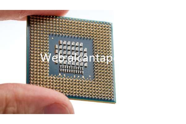
GPU基板とは?
GPU 基板 グラフィックス処理ユニットを接続およびサポートするために使用される基板を指します。 (GPU) およびその他の関連電子部品. これらの基材の主な機能は、機械的サポートを提供することです。, 電気接続, GPU の熱経路. 複雑な多層構造により、, GPU 基板は、信号伝送の完全性と電源の安定性を確保しながら、限られたスペースで高密度の電気的相互接続を実現できます。.
現代の電子機器では, GPU は、高性能のグラフィックス処理とコンピューティングを可能にするコア コンポーネントです。. ゲームにおけるグラフィックス処理能力の需要として, バーチャルリアリティ, 人工知能などの分野は増え続けている, GPU のパフォーマンス要件もますます高くなっています. これは、GPU チップ自体に高い要件を課すだけではありません, しかし、パッケージ基板にも厳しい性能基準を課しています。. 多層設計と高熱伝導性材料の適用により, GPU 基板は GPU の放熱性能を効果的に向上させ、高負荷ワークロード下でも安定して動作できるようにします。.
加えて, GPU 基板は機械的強度と信頼性の要件も満たす必要があります. GPUは動作中に大量の熱と機械的ストレスを発生するため、, 基板は、熱膨張や機械的振動による構造的損傷を防ぐのに十分な強度と耐久性を備えていなければなりません。. これには、基板材料が優れた電気伝導性と熱伝導性を備えているだけでなく、, 優れた機械的特性も備えています.
これらの機能を実現するために, GPU 基板は通常、高密度有機樹脂の組み合わせを使用します。, 陶器, および金属材料. これらの材料は、多層積層などの高度な製造プロセスを通じて複雑な多層回路構造を形成します。, 電気メッキとエッチング. 回路の各層は電気接続のためだけに使用されるわけではありません, 放熱と信号シールドの目的でもあります, これにより、複雑な作業環境における GPU の安定性と信頼性が確保されます。.
全体, GPU 基板は、最新の高性能コンピューティングおよびグラフィックス処理デバイスにおいて重要な役割を果たします。. 最適化された設計と先進材料の適用により, これらの基板は、GPU の全体的なパフォーマンスを向上させるだけではありません。, グラフィックス処理技術の継続的な進歩も促進します.
GPU 基板設計リファレンス ガイド
GPU 基板の設計は、一連の厳密な設計ガイドラインと標準に従う必要がある、複雑かつ繊細な作業です。. 初め, 素材選びはデザインの基本. GPU基板には通常、高密度の有機樹脂が使用されます (FR-4など), セラミックスや金属材料. これらの材料は、優れた電気伝導性と熱伝導性を備えている必要があるだけではありません。, しかし、高温環境でも安定性を保つ必要もあります. 酸化アルミニウムや窒化アルミニウムなどのセラミック材料は、高性能GPUに広く使用されています 包装基板 熱伝導率が高く、電気絶縁性に優れているため.
第二に, 多層構造設計がGPU基板の核心. 多層設計により、効率的な熱放散経路を提供しながら、限られたスペースで高密度の電気相互接続が可能になります。. 信号伝送の完全性と配電の安定性を確保するには、各層の回路レイアウトと配線設計を正確に計算してシミュレーションする必要があります。. 高周波信号処理用, 設計者は、信号の反射と放射損失を減らすために、配線のインピーダンス整合とシールド設計に特別な注意を払う必要があります。.
設計の精度と信頼性を確保するため, 設計者は通常、高度な設計ツールとシミュレーション ソフトウェアを使用します。. これらのツールは、さまざまな動作条件下での基板の挙動をシミュレートできます。, デザイナーが潜在的な問題を特定して解決できるように支援する. 例えば, 電磁シミュレーション ソフトウェアは、基板上の信号の伝送をシミュレートし、起こり得る干渉と損失を分析できます。. 熱シミュレーション ソフトウェアは基板の熱分布をシミュレーションし、設計者が放熱設計を最適化するのに役立ちます。.
加えて, 機械的強度と信頼性のテストも設計プロセスの重要な側面です. GPUは動作中に大量の熱と機械的ストレスを発生するため、, 基板は、熱膨張や機械的振動によって引き起こされる構造的損傷を防ぐために、十分な機械的強度と耐久性を備えていなければなりません。. 一般的な試験方法には機械的強度試験が含まれます, 熱サイクル試験と老化試験. これらのテストでは、実際の使用時に基板の潜在的な問題を特定し、さまざまな動作条件下で安定して動作できることを確認できます。.
ついに, 品質管理は設計プロセスでも重要です. 厳格な品質管理基準とプロセスにより、各基板の性能と信頼性が保証されます。. デザイナーは詳細な品質管理基準とプロセスを開発する必要がある, 材料検査も含めて, 生産工程管理, そして完成品検査. 徹底した品質管理により, 製造不良率が大幅に減少し、製品の全体的な品質が向上します。.
総括する, GPU 基板の設計には、複数の要素を総合的に考慮する必要があります, 素材選びから, 構造設計から性能試験、品質管理まで. 各リンクには綿密な設計と厳密な制御が必要です. 一連の設計ガイドラインと標準に従うことにより、, 設計者は、優れたパフォーマンスと高い信頼性を備えた GPU パッケージ基板を開発できます。, 最新の高性能コンピューティングおよびグラフィックス処理装置に強固な基盤を提供します.
GPU基板に使用されている材料?
GPU 基板の材料選択は重要です. これらの材料の選択と適用は性能に直接影響します。, 基板の信頼性と製造プロセス. 以下は、GPU 基板で一般的に使用される材料とその用途と特性です。.
初めに, FR-4などの有機樹脂材料が最も一般的な基板材料です. FR-4は機械的強度と電気絶縁性に優れたガラス繊維強化エポキシ樹脂材料です。. 熱や化学腐食に強いだけではありません, 安定した電気的性能も提供します, さまざまな電子製品の基板製造に広く使用されています。. GPU基板用, FR-4 は配合とプロセスを改善することで、機械的および電気的特性を維持しながら厚さをさらに薄くすることができます。.
セラミック材料も GPU 基板の重要な選択肢です. 一般的に使用されるセラミック材料には酸化アルミニウムが含まれます (Al2O3) そして窒化アルミニウム (AlN). これらの材料は非常に高い熱伝導性と電気絶縁性を備えています。, 高温環境でも安定して動作します。. 酸化アルミニウムは優れた機械的特性を持ち、コスト効率が高い, 一方、窒化アルミニウムは熱伝導率と電気特性が高いため、より要求の厳しい用途に適しています。. 極薄基板の設計において, セラミック材料は基板の放熱能力を効果的に向上させ、GPUの安定した動作を保証します。.
金属材料, 銅や銅合金など, 主にGPU基板の導電層と放熱層に使用されます。. 銅は電気伝導性と熱伝導性に優れており、電気信号を効果的に伝え、熱を放散します。. 基板製造において, 電気めっきとエッチングのプロセスは、基板上および基板内に正確な導電パターンを形成するためによく使用されます。. 高性能アプリケーション向け, 銅合金は、合金元素の導入により銅の機械的強度と疲労耐性を向上させるために使用することもできます。.
近年では, グラフェンなどの新素材もGPU基板に使用され始めている. グラフェンは、炭素原子の単層で構成される二次元材料であり、非常に高い導電性を持っています。, 熱伝導率と機械的強度. その独特の物理的および化学的特性により、グラフェンは極薄基板に大きな応用可能性をもたらします。. 例えば, 基板材料にグラフェンを添加することで, 基板の熱伝導率と電気的性能を大幅に向上させることができます。, 厚さを減らすことができます, 機械的強度を高めることができます.
加えて, 基板の性能と信頼性をさらに向上させるために, 設計者はさまざまな複合材料や構造を使用します。. 例えば, 有機樹脂材料にセラミック粉末を配合, 有機材料の柔軟性とセラミック材料の高熱伝導性を併せ持つ基板が得られます。. 同様に, 多層構造設計による, さまざまな材料の利点を基板に統合できる, 外層に高導電性素材、中間層に高強度素材を採用するなど, これにより、パフォーマンスの最適なバランスが実現されます。.
これらの材料を選択して適用する場合, 複数の要素を考慮する必要がある, 材料の機械的特性を含む, 電気的特性, 熱伝導率, 料金, そして加工技術. 例えば, 高い熱伝導性と信頼性が必要な用途向け, ハイパフォーマンスコンピューティングやデータセンターなど, セラミックやグラフェンなどの高性能材料が好ましい場合もあります. 家電製品向け, コストや加工性をより考慮し、最適な有機樹脂材料を選択できます.
全体, GPU 基板の材料選択は複雑かつ重要なプロセスです. さまざまな高機能素材を合理的に選択・組み合わせることにより、, 基材は機械的強度の点で最高の性能を達成できます。, 電気性能, および熱管理, さまざまなハイエンド電子機器のニーズに応えます。.
GPU基板のサイズはどれくらいですか?
GPU 基板のサイズと形状はアプリケーションのニーズに応じて異なります, そして厚さ, 長さ, これらの基板の幅は、特定の GPU パッケージとアプリケーション環境に基づいてカスタマイズする必要があります。. 以下は、GPU 基板のサイジング設計の詳細な調査です。.
初め, 基板の厚さは重要なパラメータです. 通常, GPU 基板の厚さは数百ミクロンから数ミリメートルの範囲です. 具体的な厚さの選択はさまざまな要因によって決まります。, 機械的強度も含めて, 電気特性と放熱能力. ポータブルデバイス向け, スマートフォンやタブレットなど, 設計者はデバイス全体のサイズと重量を減らすために、できるだけ薄い基板を選択する傾向があります。. しかし, 基材が薄すぎると機械的強度が不足し、使用中に容易に曲がったり破損したりする可能性があります。. したがって, 設計プロセス中に, 正確な計算とシミュレーションにより、厚さと強度の最適なバランスポイントを見つける必要があります.
基板の厚みを決めたら, 基板の長さと幅も特定の用途に応じて設計する必要があります. さまざまな GPU パッケージ サイズとレイアウト要件が基板のフォーム ファクターに影響します. 一般的に言えば, 基板の長さと幅は、GPU パッケージおよびその他の必要な電子コンポーネントを完全にカバーできる必要があります。, 信号ルーティングと電力分配のために適切なスペースを残します。. 加えて, 基板の形状は、組み立て中に他のコンポーネントとしっかりとフィットするように、デバイスの外部デザインと一致する必要もあります。.
設計の柔軟性と適応性を向上させるため, GPU 基板のサイズ設計は通常、モジュール式のカスタマイズされたアプローチを採用します。. モジュラー設計により、設計者はさまざまなアプリケーションのニーズに応じてさまざまなサイズや形状のベースボード モジュールを選択して組み合わせることができ、最適なパフォーマンスとコスト効率を実現できます。. カスタマイズされた設計は、特定のプロジェクトの特別なニーズに基づいています, 特定のアプリケーションの要件を満たす特殊なサイズとレイアウト設計を備えています.
配線密度もサイジングの重要な考慮事項です. 電子機器の高機能化が進む中、, 基板上の電子部品と接続ポイントの数も同様です. 設計者は、信号伝送の安定性と配電の信頼性を確保するために、限られた基板面積上にこれらのコンポーネントと接続ポイントを合理的にレイアウトする必要があります。. この目的を達成するために, 配線経路と層間接続を最適化することで配線密度と基板の集積度を向上させるには、高度な配線技術と設計ツールを使用する必要があります。.
加えて, 基板のサイズ設計は製造プロセスやコストも考慮する必要があります. 過度に複雑で正確な寸法設計は、製造の困難さとコストを増加させる可能性があります, 最終製品の経済性に影響を与える. 設計者は、プロセスの最適化とコスト管理を通じて、パフォーマンスとコストの最適なバランスを見つける必要があります。. 例えば, 設計プロセス中に, 標準化されたサイズとテンプレートを使用して、生産プロセスの複雑さとばらつきを軽減し、生産効率と歩留まりを向上させることができます。.
実際のアプリケーションでは, GPU 基板のサイズ設計にも一連のテストと検証が必要です. 物理サンプルの製造とテストを通じて, 設計の実現可能性と信頼性を検証できる, 潜在的な問題を発見して解決できる. 一般的な試験方法には機械的強度試験が含まれます, 電気性能試験, 熱サイクル試験, 等. これらのテストは、実際の使用における基板の性能と信頼性を保証し、さまざまな動作条件のニーズを満たすことができます。.
一般的に, GPU 基板のサイズ設計は、機械的性能などの複数の要素を総合的に考慮する必要がある複雑かつ重要なプロセスです。, 電気性能, 放熱能力, 製造工程とコスト. 適度なサイズ設計により、, 基板の性能と経済性の最適なバランスを実現し、さまざまなハイエンド電子機器のニーズに対応します。.
GPU基板の製造工程
GPU基板の製造プロセスは複雑かつ精密です, 完了するまでに複数のプロセスが必要になる. 最終製品の品質と性能を確保するには、各プロセスで厳密な制御と最適化が必要です。. 以下は GPU 基板の製造プロセスの詳細な説明です。.
まず、基板材料の選択と準備です。. 設計要件に従って, 適切な有機樹脂を選択する, セラミックまたは金属素材. 材料の選択は、機械的および電気的特性だけを考慮する必要はありません, 処理性能とコストも. 素材を選んだあとは, 大きな材料片を指定されたサイズと形状の基板ブランクに切断するには、切断と成形が必要です. このプロセスでは通常、高精度の切断装置が使用されます。, レーザーカッターやCNCカッターなど, 基板寸法の精度と一貫性を確保するため.
次はラミネートとラミネートの工程です. 多層基板設計向け, 多層の導電パスを備えた複合基板を形成するには、複数の材料層を積み重ね、高温高圧でプレスする必要があります。. ラミネート加工中, 温度, 材料のさまざまな層間の緊密な接着と電気的接続を確保するには、圧力と時間を厳密に制御する必要があります。. このプロセスは通常、空気や不純物の混入を避けるために真空環境で行われます。, 基板の性能と信頼性に影響を与える可能性があります.
ラミネート完了後, 基板に穴を開けて電気メッキする必要があります. 電気接続経路を作成するために穴あけプロセスが使用されます。, スルーホールや止まり穴など, 基板上に. このプロセスでは通常、高精度の穴あけ装置が使用されます。, 機械的穴あけまたはレーザー穴あけによる, 穴の位置とサイズの精度を確保するため. 電気めっきプロセスでは、基板表面と穴壁に銅またはその他の導電性材料の層をコーティングして、電気接続経路を形成します。. このプロセスは、コーティングの厚さと均一性を確保するために、厳密なプロセスパラメータの下で実行する必要があります。.
続いてフォトリソグラフィーとエッチングのプロセスが行われます。. フォトリソグラフィープロセスでは、フォトリソグラフィー技術を使用して、基板の表面に必要な回路パターンを形成します。. 初め, 感光性材料の層が基板の表面にコーティングされます, その後、フォトマスクを介してパターンを感光性材料に露光します。. 曝露後, 感光材料の感光部分が現像液によって溶解される, 希望のパターンを残す. エッチングプロセスでは、化学エッチング液を使用して余分な材料を除去します。, 感光性材料によって保護された導電パスを残す. このプロセスでは、パターンの精度と導電パスの完全性を確保するために、エッチング時間とエッチング液の濃度を厳密に制御する必要があります。.
フォトリソグラフィーとエッチングが完了した後, 基板も一連の洗浄を受ける必要があります, テストとパッケージングのプロセス. 洗浄プロセスは、基板表面の残留物や汚染物質を除去し、基板の清浄度と性能を確保するために使用されます。. 試験プロセスでは、電気性能試験を通じて基板の性能と信頼性を検証します。, 機械的強度試験, 熱サイクル試験およびその他の方法. パッケージングプロセスでは、基板と他の電子コンポーネントを組み立てて、完全な電子モジュールまたはデバイスを形成します。.
製造工程の安定と製品の品質を確保するため, 製造業者は通常、高度な製造装置とプロセス制御システムを採用しています. 例えば, 自動化された生産ラインは、生産効率と一貫性を向上させ、手動操作によって引き起こされるエラーとばらつきを減らすことができます。. オンライン検出および監視システムは、生産プロセスの主要なパラメータをリアルタイムで監視できます。, 潜在的な問題をタイムリーに発見して修正する, 各プロセスの品質と安定性を確保します.
加えて, 製造プロセスの最適化と改善も、製品の品質を向上させ、生産コストを削減する重要な方法です。. 継続的なプロセス改善と技術革新を通じて, 製造効率と製品のパフォーマンスを向上させることができます, 生産コストとスクラップ率を削減できます. 例えば, より効率的な材料とプロセスを使用する, プロセスフローとパラメータの最適化, 高度な検出および制御技術の適用はすべて、製造プロセスを最適化するための重要な手段です.
一般的に, GPU基板の製造プロセスは複雑かつ精密です, 材料の選択など複数の側面を総合的に考慮する必要がある, プロセス制御, 機器のアプリケーション, と品質管理. 厳格な管理と継続的な最適化を通じて, さまざまなハイエンド電子機器のニーズを満たす最終製品の品質と性能を確保できます。.
GPU基板の応用分野
GPU 基板には幅広い用途があります, 優れた性能とデザインにより、現代の電子機器に広く使用されています。. 以下に主な応用分野と具体的な例を示します。.
初め, GPU 基板はハイパフォーマンス コンピューティングで広く使用されています. 例えば, サーバーとデータセンターは、大量のデータと複雑なコンピューティングタスクを処理する必要があります, 基板の電気的性能と放熱能力に対して非常に高い要件が求められます。. GPU 基板は、優れた電気性能と高い熱伝導率により、サーバーやデータセンターのコンピューティング効率と安定性を向上させることができます。. 人工知能アクセラレータと高性能コンピュータにおいて, GPU 基板は、高密度配線と高伝導性を通じて効率的な信号伝送と電力分配を提供し、複雑なコンピューティングおよびデータ処理タスクをサポートします。.
ゲームや仮想現実デバイスにおいて, GPU基板も重要な役割を果たします. これらのデバイスには、グラフィックス処理能力に対する非常に高い要件があります。. GPU 基板は、高密度の相互接続と効率的な熱放散により、高負荷ワークロード下でも GPU の安定性とパフォーマンスを保証します。. ゲーム機やハイエンドグラフィックスワークステーションで, GPU 基板は、優れたグラフィックス処理機能とスムーズなユーザー エクスペリエンスを提供します。.
加えて, GPU基板は自動車エレクトロニクスや産業用制御の分野でも広く使用されています. 自動車エレクトロニクス分野, GPU 基板は先進運転支援システムをサポートするために使用されます (ADAS), 車載エンターテインメントシステムと自動運転技術. これらのアプリケーションには、基板の信頼性と耐久性に関する厳しい要件があります。, および GPU 基板は、優れた機械的および電気的特性により、自動車エレクトロニクスの高い基準を満たしています。. 産業用制御機器において, GPU 基板は、複雑な制御およびデータ処理タスクをサポートするために使用されます。, 生産効率とシステムの安定性の向上.
GPU基板の利点は何ですか?
GPU (グラフィックス処理装置) パッケージ基板は、現代のコンピューター グラフィックス処理と科学計算において重要な役割を果たしています。. GPU動作をサポートするプラットフォームだけではありません, だけでなく、パフォーマンスの安定性と信頼性を確保する上でも重要な部分です. GPU パッケージ基板の主な利点は次のとおりです。:
優れた放熱性能: GPU パッケージ基板の設計では、高性能コンピューティングのニーズが考慮され、最適化された熱放散ソリューションが提供されます。. 効果的な放熱設計により, GPU パッケージ基板は、高負荷動作中に良好な温度制御を維持できます。, 過熱による性能低下や機器の損傷を防ぎます。.
最適化された電気的性能: 高速プロセッサのメインサポートプラットフォームとして, GPU パッケージ基板には高度な電気設計が採用されており、安定した信号伝送と最小限の電磁干渉を保証します。. この最適化により、システム全体のパフォーマンスが向上します。, データ送信の遅延を削減する, グラフィックスおよびコンピューティングタスクの処理効率を向上させます。.
多用途性と柔軟性: GPU パッケージ基板は多くの場合、柔軟性があり、さまざまなサイズや形状の GPU チップをサポートするように設計されています。. この柔軟性により、GPU パッケージ基板はさまざまなアプリケーションに適しています, デスクトップ コンピュータやゲーム コンソールからデータ センターやスーパーコンピュータまで.
高密度かつコンパクトな設計: 現代の機器の小型化・高性能化のニーズに応えるために, GPUパッケージ基板は高密度レイアウト設計を採用. この設計により、限られたスペースでより多くの電子コンポーネントとコネクタを統合することが可能になります。, 装置の小型化・軽量化を実現.
信頼できる製造プロセス: GPU パッケージ基板の製造プロセスは、高水準のプロセス フローに厳密に従っています, 素材選びも含めて, ラミネート加工, 回路基板の設計と組立技術. これらにより、GPU パッケージ基板の品質と信頼性が保証され、製造時の故障率とメンテナンスコストが削減されます。.
要約すれば, GPU パッケージ基板は、最適化された熱的および電気的パフォーマンスを提供するだけではありません, 多用途性も備えています, 高密度設計と信頼性の高い製造プロセス. これらの利点により、GPU パッケージ基板は現代のコンピュータ グラフィックス処理と科学計算に不可欠な部分となっています。, 技術の継続的な進歩と用途の拡大を促進する.
よくある質問
GPU 基板に使用されている材料?
通常, GPU基板はFR4を使用 (グラスファイバー強化エポキシラミネート) 主な材料として. この材料は優れた電気絶縁特性と機械的強度を備えています。, 高性能コンピューティング環境での安定した動作に適しています。.
GPU 基板の寸法はどのくらいですか?
GPU 基板のサイズはアプリケーションによって異なります. ラップトップ GPU と同じくらい小さくても、サーバークラスの GPU と同じくらい大きくてもよい. サイズは通常、GPU チップのサイズと熱要件によって決まります。.
GPU基板の製造プロセスとは何ですか?
GPU 基板の製造プロセスには基板の準備が含まれます, 銅層の堆積, フォトレジストの塗布と露光, エッチング, 掘削, コンポーネントの取り付け, はんだ付けとテスト. 最終製品の品質と信頼性を確保するために、各ステップは厳密に管理されています.
GPU 基板の応用分野は何ですか?
GPU 基板はゲーム グラフィック カードで広く使用されています, データセンターサーバー, 人工知能コンピューティング, 科学計算, 仮想現実およびその他の分野. これらは、高性能グラフィックスとコンピューティングのニーズを実現するための重要なコンポーネントです。.