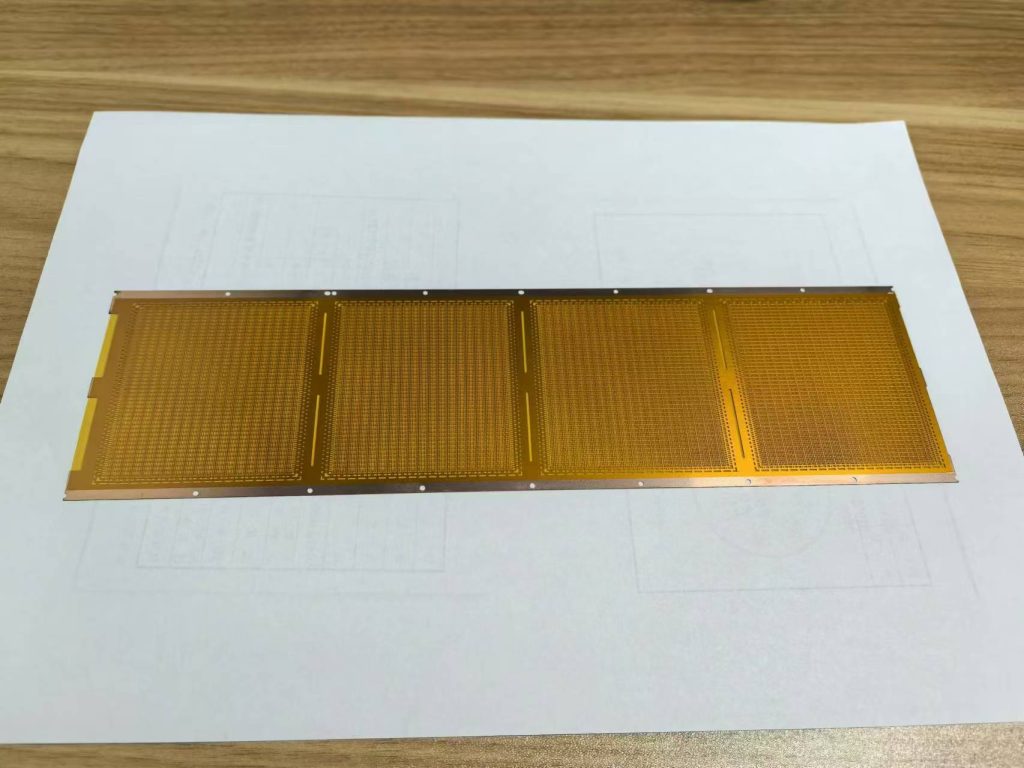
について 接触 |
電話番号: +86 (0)755-8524-1496
Eメール: info@alcantapcb.com

QFNパッケージメーカー向けリードフレーム, QFN Metal frame 生産, QFNメタルフレームの表面処理に銀メッキまたはAuメッキを施しております。, about the silver and Au thickness, We will plating thickness according to your requirement.

In the world of semiconductor packaging, the lead frame plays a crucial role, particularly in QFN (Quad Flat No-lead) パッケージ. With the increasing demand for miniaturization and enhanced performance in electronic devices, QFN packages have become a popular choice due to their compact size, thermal performance, and cost-effectiveness. The lead frame is a key component in this packaging process, providing both mechanical support and electrical connectivity. This article delves into the significance of the lead frame in QFN packages, highlighting its design, advantages, and manufacturing process.

What is a Lead Frame?

A lead frame is a metal structure, typically made from copper or a copper alloy, that forms the backbone of many IC (集積回路) パッケージ. In the context of QFN packaging, the lead frame serves several critical functions. It provides a foundation for mounting the semiconductor die, connects the die to external circuits, and helps manage heat dissipation. Unlike traditional IC packages with protruding leads, the QFN package utilizes a flat, leadless design, where the connections are located at the bottom of the package, making it more compact and efficient.

QFNパッケージ用リードフレーム
QFNパッケージ用リードフレーム

The Role of Lead Frames in QFN Packages

In QFN packages, the lead frame plays two primary roles: mechanical and electrical.

1. Mechanical Support

The lead frame serves as the base upon which the semiconductor die is mounted. After the die is attached, the lead frame ensures structural integrity during subsequent processing steps, such as wire bonding and encapsulation. さらに, the exposed pad in the QFN package, which is part of the lead frame, plays a significant role in improving heat dissipation. This is crucial in high-power applications, where maintaining thermal performance is essential to ensuring reliability and longevity of the device.

2. Electrical Connectivity

The lead frame also serves as the primary conduit for electrical signals between the semiconductor die and external circuits. In a QFN package, the electrical connections between the die and the lead frame are established using wire bonding or flip-chip bonding. These connections are then routed through the lead frame to the bottom of the package, where they interface with the PCB (プリント基板). This design ensures a low-inductance path for high-frequency signals, making QFN packages suitable for high-speed applications.

Advantages of Lead Frame-Based QFN Packages

There are several advantages to using lead frame-based QFN packages:

  1. Compact Size: QFN packages are much smaller than traditional leaded packages, making them ideal for portable and space-constrained applications. The use of lead frames enables efficient space utilization without sacrificing performance.
  2. Thermal Performance: The exposed pad on the bottom of the QFN package, which is part of the lead frame, provides a direct path for heat dissipation. This is especially important in high-power applications, as it helps manage heat more effectively than traditional packages.
  3. Cost-Effective: Lead frames are relatively inexpensive to manufacture and offer a cost-effective solution for mass production. さらに, the simplicity of the QFN design reduces the complexity of assembly, further lowering costs.
  4. High Electrical Performance: The lead frame’s ability to provide low-inductance electrical connections ensures that QFN packages can support high-speed and high-frequency applications with minimal signal loss.

Manufacturing Process

The manufacturing of lead frames typically involves stamping or etching metal sheets, followed by plating to improve corrosion resistance and electrical conductivity. The lead frame is then integrated into the QFN package during assembly, where the semiconductor die is attached to the lead frame, wire bonding is performed, and the package is encapsulated with a protective molding compound. After molding, the package is trimmed and formed to expose the lead frame’s electrical terminals at the bottom, completing the QFN assembly.

結論

The lead frame is an essential component in QFN packaging, providing mechanical support, electrical connectivity, and thermal management. Its simple yet effective design makes it a cornerstone of modern semiconductor packaging, especially in applications that demand miniaturization and high performance. 電子機器が進化し続ける中、, the role of lead frame-based QFN packages will only grow, offering manufacturers a reliable and cost-effective solution for a wide range of applications.

前へ:

次:

返信を残す

このサイトはスパムを低減するために Akismet を使っています. コメントデータがどのように処理されるかをご覧ください.