株式会社")
進化し続ける半導体パッケージング技術の世界, 効率的で信頼性の高い設計が現代のエレクトロニクスを駆動する鍵となります. 半導体パッケージングには、外部回路へのシームレスな電気接続を確保しながら保護するために繊細なチップをカプセル化することが含まれます。. さまざまなパッケージング技術の中から, チップパッケージ上のリードフレームは重要なコンポーネントです.
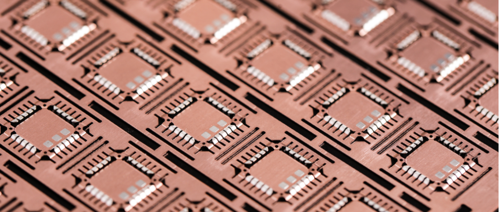
チップ パッケージ上のリードフレームは、チップ接続のバックボーンとして機能する薄い金属構造です。, 半導体チップと外部デバイスの間のギャップを埋める. 導電性を確保します, 構造的サポート, そして放熱, 多くのアプリケーションで不可欠なものとなっています.
リードフレームオンチップパッケージとは?
チップパッケージ上のリードフレームは、 半導体パッケージ, 機械的サポートを提供し、半導体ダイ間の電気的接続を確立するように設計されています。 (チップ) および外部回路. リードフレームは薄い金属構造物です, 通常は銅または銅合金で作られています, チップの統合と接続を容易にする、正確にエッチングまたはスタンプされたパターンを備えています. チップパッケージに組み込む場合, リードフレームは、チップの小さな内部回路をより大きな回路に接続するインターフェースを形成します。, プリント基板などの外部システム (プリント基板).
チップパッケージ上のリードフレームの主な機能は 2 つあります。: 半導体ダイを実装するための安定したプラットフォームを提供し、ダイと外部回路の間で電気信号をシームレスに伝達します。. この二重の役割により、外部損傷から物理的に保護されながら、チップが効率的に動作することが保証されます。. さらに, リードフレームは、動作中にチップから発生する熱を放散するのに役立ちます。, デバイスの信頼性の向上.
リードフレームオンチップパッケージは、いくつかのパッケージタイプで共通の機能です, 含む QFN (Quad Flat No-Lead), 浸漬 (デュアルインラインパッケージ), およびSOP (スモールアウトラインパッケージ). これらのパッケージ スタイルはそれぞれ、サイズのバランスをとるためにリード フレームを利用しています。, 料金, とパフォーマンス. 例えば, QFNパッケージ, リードの突出がないリードフレームを採用, コンパクトで広く使用されています, 高性能エレクトロニクス. その適応性により、リード フレーム オン チップ パッケージはさまざまな用途で好ましい選択肢となります。, 家庭用電化製品から自動車および産業システムまで.
チップパッケージ用リードフレーム材料: 何が効果的なのか?
リードフレームオンチップパッケージの材料の選択は、その性能を決定する重要な要素です。, 耐久性, そして 製造業 実現可能性. 一般的に使用される材料には銅が含まれます, 銅合金, 場合によってはアルミニウムや鉄ニッケル合金などの他の金属も使用されます。. 銅は優れた導電性を備えているため、最も普及しています。, 熱性能, 比較的手頃な価格. 銅合金, 多くの場合、鉄やニッケルなどの元素で強化されています, 機械的強度と耐酸化性が向上します。, より要求の厳しい用途に適したものにする.
材料の選択は、3 つの重要な特性に直接影響するため、チップ パッケージ上のリード フレームにとって非常に重要です。:
- 電気伝導率: 高い導電率により、チップと外部回路間の効率的な信号伝送が保証されます。, エネルギー損失を最小限に抑える.
- 耐久性: 材料は組み立て中の物理的ストレスに耐える必要があります, ワイヤーボンディング, そして長期運用.
- 熱性能: 効果的な熱放散は、チップの信頼性を維持し、動作中の過熱を防ぐために重要です。.
リードフレームオンチップパッケージの製造工程において, 選択した材料に精密なエッチングまたはスタンピングを施し、チップの設計に合わせた複雑なパターンを形成します。. 形成後, リードフレームは銀などの材料でメッキされています, 金, またはパラジウムで導電性を高め、腐食から保護します. これらのプロセスは、材料の特性が製造の容易さと精度にどのような影響を与えるかを浮き彫りにします。.
素材を厳選し加工することで、, メーカーはコストのバランスをとったチップパッケージ上にリードフレームを作成できる, パフォーマンス, そして長寿, それらは現代の電子機器に不可欠なものとなっています.
チップパッケージのリードフレーム製造プロセス
リードフレームオンチップパッケージの製造プロセスには、機能を確保するための複数の正確なステップが含まれます, 耐久性, コスト効率. 各段階は、半導体パッケージングの厳しい要件を満たす高品質のリードフレームを製造するために慎重に設計されています。. 段階的なプロセスの詳細は次のとおりです:
1. 材料の選択と準備
プロセスは適切な材料を選択することから始まります, 通常は銅または銅合金, 優れた導電性により, 熱放散, および機械的特性. 選択した材料は、その後の製造ステップを容易にするために、薄いシートまたはストリップとして準備されます。. この段階で均一性と品質を確保することは、チップパッケージ上に信頼性の高いリードフレームを製造するために重要です。.
2. エッチングとスタンピング
材料が準備できたら, チップ設計に合わせた複雑なパターンを 2 つの方法のいずれかを使用して作成します:
- エッチング: 化学エッチングプロセスを使用して不要な材料を溶解します, 望ましいパターンを残す. この方法は複雑な設計に最適であり、高精度を実現します。.
- スタンピング: 機械的スタンピングプロセスでは、金型を使用して必要なパターンを打ち抜きます。. このアプローチは、単純な設計では高速かつコスト効率が高くなりますが、エッチングで達成できる微細なディテールが欠けている可能性があります。.
これらのプロセスにより、チップ パッケージ上のリード フレームの基本構造が形成されます。, 外部接続用のダイアタッチパッドとリードを含む.
3. リードのメッキとフォーミング
リードフレームのパターニング後, 銀のような材料の薄い層でメッキされています, 金, または導電性を向上させるパラジウム, 酸化を防ぎます, 結合性を高める. 一部のアプリケーションには、はんだ付け性を高めるために錫めっきが必要です.
その後、リードは機械的に最終形状に成形されます。, 特定のチップパッケージ設計との互換性を確保する. このステップは、チップ パッケージ上のリード フレームを使用するデバイスで堅牢な電気接続を作成するために不可欠です。.
4. QFNの製造 (Quad Flat No-Lead) リードフレームオンチップパッケージ
QFN リードフレームはリードレス設計のため、さらなる精度が必要です, 電気接点がパッケージの底部で直接露出している場合. 製造工程で重視しているのは、:
- 精密なリード構造を実現するための超微細エッチングまたはスタンピング.
- 強化されたメッキにより、組み立て中の信頼性の高いはんだ付けが保証されます.
- 平面度を維持し、反りを防ぐための厳格な品質管理, QFN のコンパクトで高性能なアプリケーションにとって重要です.
5. 主要な課題と技術の進歩
チップパッケージ上のリードフレームの製造はいくつかの課題に直面しています, のような:
- 材料廃棄物: エッチングまたはスタンピングプロセス中のスクラップを最小限に抑える.
- 精度の要件: チップの縮小が続く中、マイクロスケールのパターンの一貫性を確保.
- 環境への懸念: エッチングおよびメッキプロセスにおける有害な化学物質の使用を削減.
最近の進歩, レーザー支援による製造など, 改良されためっき技術, 環境に優しい化学プロセス, これらの課題に対処する. 自動化と AI を活用した品質管理システムにより、リードフレーム生産の効率と精度も向上しました.
これらの詳細な手順に従うことで、, メーカーは、最新の半導体アプリケーションの厳しい基準を満たすチップ パッケージ上のリード フレームを製造しています。, エレクトロニクス業界の高性能化と小型化への取り組みをサポート.
チップパッケージ上のリードフレームとワイヤボンディング
ワイヤボンディングは半導体パッケージングにおける重要なステップです, チップパッケージ上のリードフレームを介してチップの内部回路を外部世界に直接接続します。. このプロセスには、細いワイヤーを使用して超微細な電気接続を作成することが含まれます。, 通常は金で作られています, アルミニウム, または銅. これらのワイヤは、半導体ダイ上のボンドパッドをリードフレームのリードに接続します。, 信号伝送と電力供給を可能にする.
チップパッケージ上のワイヤボンディングとリードフレーム: つながり
チップパッケージ上のリードフレーム内, リードフレームはワイヤボンディングのための構造化されたプラットフォームを提供します. ダイ上のボンディング パッドはリード フレーム上のボンディング ポイントと正確に位置合わせされます。, 正確で安定した接続を確保する. リードフレームの堅牢な設計は、その後のパッケージング段階で繊細なワイヤを保護しながら、ワイヤボンディングプロセスをサポートします。.
チップパッケージ上のリードフレームにワイヤを取り付けるプロセス
ワイヤーボンディングは複数の段階で行われます:
- 金型の配置: 半導体ダイは、接着剤またははんだを使用してリードフレームのダイ取り付けパッドに取り付けられます。.
- ワイヤーボンディングのセットアップ: ワイヤボンディングマシンは、顕微鏡下でダイとリードフレームの位置を調整し、精度を確保します。.
- 絆の形成: 細いワイヤがボンディング ツールに通され、次のいずれかの手法を使用してダイのボンド パッドに取り付けられます。:
- 熱音波接着: 熱を組み合わせる, 超音波エネルギー, 強いつながりを築くというプレッシャー (金線によく使われる).
- 超音波接合: 熱を使わずに超音波振動を利用する, アルミ線に最適.
- 熱圧着: 熱と圧力による接着, 通常は高信頼性アプリケーション向け.
- ワイヤーループとセカンドボンド: ボンディング ツールはワイヤをリード フレーム上の対応するリードにループさせ、2 番目のボンドを形成します。, 接続を完了する.
このプロセスはチップ上のすべてのボンドパッドに対して繰り返されます。, すべての内部回路がリードフレームの外部リードに確実に接続されるようにする.
チップパッケージ上のリードフレームのワイヤボンディングに関する重要な考慮事項
- アライメント精度: ワイヤボンディング中の位置ずれは、ショートや接続不良を引き起こす可能性があります. 高精度の機械と堅牢なリードフレーム設計により、完璧な位置合わせが保証されます.
- 社債の信頼性: ワイヤボンドは機械的ストレスに耐える必要があります, 熱サイクル, デバイスのライフサイクルにおける環境要因. 線材の適切な選択, 接着方法, リードフレーム上のメッキにより接合の完全性が保証されます.
- 材質の適合性: ワイヤとリードフレームのメッキ材料は、腐食や金属間化合物の形成を避けるために適合性がある必要があります。, 接続が低下する可能性があります.
- ループのプロファイルと長さ: ワイヤ ループの高さと長さは、カプセル化または隣接するコンポーネントとの干渉を避けるために最適化する必要があります。.
ワイヤボンディングはチップパッケージ上のリードフレームの機能において重要な役割を果たします, チップ回路の微視的スケールと外部システムの巨視的インターフェースの橋渡し. その精度と信頼性は、最新の電子機器のシームレスなパフォーマンスを可能にする鍵となります。.
リードフレームパッケージとは? チップパッケージにおけるリードフレームの役割
リードフレームパッケージは、リードフレームを構造的および電気的基盤として利用する半導体パッケージングの一種です。. チップパッケージ上のリードフレームは、半導体ダイと外部回路間のブリッジを形成します。, 機械的サポートを提供します, 電気接続, および熱散逸. これらのパッケージは、リードフレームとチップを保護材で包みます。, 通常は樹脂または成形材料, デバイスを環境的および機械的損傷から保護するため.
チップパッケージのリードフレームパッケージを構成するもの?
リードフレームパッケージは次の主要コンポーネントで構成されます。:
- リードフレーム: 半導体ダイを外部回路に接続するリード付きの金属フレームワーク.
- ダイアタッチパッド: チップが搭載される中央プラットフォーム, サポートと熱放散の提供.
- ボンディングワイヤー: チップのボンドパッドをリードフレームのリードに接続する細いワイヤ.
- 封止材: リードフレームとチップを包み込み、外部要因から保護するモールドコンパウンド.
リードフレームパッケージはそのシンプルさから広く使用されています, 費用対効果, さまざまな組立工程への対応.
リードフレームパッケージの種類
いくつかのタイプのリード フレーム パッケージは、リード フレーム オン チップ パッケージの利点を活用しています. これらには以下が含まれます:
- QFN (Quad Flat No-Lead):
- パッケージの底部にリードフレームコンタクトが露出しているのが特徴です.
- コンパクトなサイズで知られています, 優れた熱性能, そして高い信頼性.
- スマートフォンやIoTデバイスなどのスペースに制約のあるアプリケーションに最適.
- LQFP (薄型クアッドフラットパッケージ):
- パッケージの 4 つの側面すべてから伸びるリードが含まれています.
- ピン密度が高く、マイクロコントローラーや高速プロセッサーで一般的に使用されています。.
- 浸漬 (デュアルインラインパッケージ):
- 2 つの平行なリード列を備えた従来のリードフレーム パッケージ.
- シンプルでコスト効率が高い, スルーホール実装でよく使用されます.
- SOP (スモールアウトラインパッケージ):
- リードが2つの側面から伸びているリードフレームパッケージ.
- メモリチップや低電力デバイスで一般的.
リードフレームオンチップパッケージが半導体業界で人気がある理由
リードフレームがオン チップパッケージ いくつかの理由から依然として好ましい選択肢である:
- コスト効率: リードフレームは比較的安価に製造できる, 大量生産に適したものにする.
- 熱的および電気的性能: 銅などの高導電性素材の使用により、効率的な熱放散と信頼性の高い信号伝送が保証されます。.
- 設計の柔軟性: リードフレームオンチップパッケージは、さまざまなパッケージサイズとピン構成に対応できます, 幅広いアプリケーションをサポート.
- 小型化対応: 高度なリードフレーム設計, QFNパッケージのものなど, コンパクトを有効にする, 最新のエレクトロニクス向けの軽量ソリューション.
- 実証済みの信頼性: 堅牢な構造と確立された製造プロセスにより、耐久性と一貫したパフォーマンスが保証されます。.
リードフレームパッケージは、半導体パッケージングのための多用途かつ効率的なソリューションを代表します, 実用性と高性能を両立. その適応性と費用対効果により、あらゆる業界で不可欠なものとなっています。, 家庭用電化製品から自動車および産業用アプリケーションまで.
QFN リードフレームオンチップパッケージ: 特化したパッケージ
QFN (Quad Flat No-Lead) パッケージは、革新的でコンパクトな設計のリードフレームオンチップパッケージを組み込んだ、高度に特殊化されたタイプの半導体パッケージです。. リードが突き出た従来のパッケージとは異なります, QFNパッケージは、パッケージの底部にリードが露出しているのが特徴です。, パフォーマンスの面で独自のメリットを提供, サイズ, コスト効率.
QFN リード フレーム オン チップ パッケージの違い?
チップパッケージ上の QFN リードフレームの主な違いは、リード構造と設計です。:
- リードレス設計: リードは外側には出しておらず、パッケージ底面に露出しています。, はんだ付け中にPCBとの直接接触が可能.
- コンパクトサイズ: リードレスアーキテクチャによりパッケージの設置面積を最小限に抑えます, QFN はスペースに制約のあるアプリケーションにとって理想的な選択肢となります.
- 強化された熱性能: 露出したダイアタッチパッドと底部に取り付けられたリードにより、熱放散のための直接経路が提供されます。, 熱管理の改善.
- 電気性能の向上: 電気経路が短いため、寄生インダクタンスと寄生抵抗が低減されます。, より高速な信号伝送とより優れた全体的なパフォーマンスを保証します。.
リードフレームオンチップパッケージを備えた QFN パッケージの設計と利点
QFNパッケージの設計はシンプルさと効率を重視しています:
- ダイアタッチパッド: リードフレームの中央に配置, 半導体ダイをしっかりと保持し、多くの場合サーマルパッドとして機能します。.
- 周辺機器リード: ダイアタッチパッドの周囲, リード線はパッケージの底部にパターン化されています, 信号干渉を軽減しながら最適な接続を確保します.
- カプセル化: 全体の構造, 下のリードを除く, 環境要因から保護するためにモールドコンパウンドで覆われています.
主な利点は次のとおりです。:
- 小型化: 設置面積が小さく、プロファイルが薄いため、QFN パッケージは軽量でコンパクトなデバイスに最適です.
- 熱管理: 優れた放熱性により、過熱することなく高性能チップをサポートします.
- シグナルインテグリティ: リード長の短縮と寄生成分の低減により、高周波性能が向上.
- コスト効率: QFNパッケージはボールグリッドアレイよりも製造が簡単です (BGA) 低コストで高性能の代替品を提供します.
最新のデバイスにおける QFN パッケージのアプリケーション
リードフレームオンチップパッケージを備えた QFN パッケージは、その汎用性によりさまざまな業界で広く採用されています:
- 家電:
- スマートフォンで発見, 錠剤, およびウェアラブルデバイス, 省スペースとパフォーマンスが重要な場合.
- RFコンポーネントに最適, パワーマネジメントIC, およびマイクロコントローラー.
- 自動車システム:
- エアバッグなどの安全性が重要なシステムで使用される, エンジン制御, 信頼性と熱効率によるインフォテイメント システム.
- 産業用およびIoTデバイス:
- IoTセンサーの小型設計を可能にする, アクチュエータ, およびエッジ コンピューティング デバイス.
- 電気通信:
- ネットワーク機器の高周波アプリケーションをサポート, 無線通信モジュール, および5Gシステム.
QFN リード フレーム オン チップ パッケージは、高性能のための最先端のソリューションを表します, コンパクト, コスト効率の高い梱包ニーズ. 革新的なデザインと最新の電子機器への適応性により、幅広い用途で好まれる選択肢となっています。, テクノロジーの進歩を推進し、よりスマートなサービスを可能にする, もっと早く, そしてさらに小さい
一般的なリード フレーム オン チップ パッケージのタイプ: 特定のパッケージの探索
リードフレームオンチップパッケージは、半導体パッケージングにおいて多用途かつ不可欠なコンポーネントです, 現代の電子機器の多様な要件に合わせてカスタマイズされたバリエーション. さまざまなリードフレームのタイプ, F150など, 機能に影響を与えるユニークなデザインと特性が特徴です, 応用, とパフォーマンス.
一般的なリードフレームタイプの概要, F150を含む
- F150リードフレーム:
- 車載および高信頼性アプリケーションに最適化された特殊なリードフレーム タイプ.
- 堅牢な設計と高い熱伝導率で知られています, 過酷な環境条件や高温の動作温度に対応するのに最適です。.
- 電源管理ICで一般的に使用されています, エンジン制御モジュール, エアバッグやアンチロック ブレーキ システムなどの安全性が重要なシステム.
- 標準リードフレーム:
- DIPで広く使用されています (デュアルインラインパッケージ), SOP (スモールアウトラインパッケージ), およびQFP (クワッドフラットパッケージ) デザイン.
- 汎用用途に信頼性の高い電気接続と機械的サポートを提供します.
- QFNリードフレーム:
- 底部リードが露出したリードレス設計が特徴で、優れた熱的および電気的性能を実現します。.
- コンパクトかつ軽量, ポータブル電子機器や IoT デバイスに人気の選択肢となっています。.
- パワーリードフレーム:
- 高出力アプリケーション向けに設計, これらのリード フレームには、より高い電流負荷を処理し、熱放散を改善するために、より厚い材料とより大きなダイ取り付けパッドが組み込まれていることがよくあります。.
- パワートランジスタに使用, モスフェット, および電圧レギュレータ.
リードフレームタイプの違いとパッケージ設計への影響
- 材料の選択:
- F150 のような高性能リード フレームは、耐久性と導電性を高めるために高度な銅合金またはその他の特殊な材料を使用しています。.
- 標準リードフレームは、コスト効率の高い設計のために基本的な銅材料に依存する場合があります.
- 熱管理:
- パワーおよび QFN リード フレームには、露出サーマル パッドや最適化されたレイアウトなどの機能が組み込まれており、熱放散を改善します。.
- 標準的なリードフレームの熱処理能力は限られている場合があります, 低電力アプリケーションに適しています.
- リードの設計と構成:
- 有鉛パッケージ (例えば。, 浸漬, SOP) リードを外側に伸ばす, はんだ付けは簡素化されますが、パッケージサイズは大きくなります.
- リードレス設計 (例えば。, QFN) 寄生容量とパッケージ寸法を削減する, 高周波アプリケーションでのパフォーマンスの向上.
- アプリケーション固有の機能:
- F150 などの自動車グレードのリード フレームには、業界標準を満たすための耐食性と厳格な品質管理のための追加のメッキが組み込まれていることがよくあります。.
- コスト効率と汎用性を重視した汎用リードフレーム.
リードフレームのバリエーションがパッケージの設計と性能に与える影響
リードフレームのタイプの選択は、パッケージの熱に直接影響します。, 電気, そして機械的性能. 例えば:
- QFN リードフレームにより小型化と信号整合性が向上, ポータブル電子機器や高速電子機器にとって不可欠.
- F150 リードフレームは信頼性と堅牢性を重視, 自動車および産業システムに不可欠な.
- パワーリードフレームにより効率的な放熱が保証されます, 高電力回路のコンポーネントの寿命を延ばす.
メーカーはアプリケーション固有の要件に基づいてリードフレームのタイプを選択します, パフォーマンスのバランス, 料金, と信頼性. この適応性は、多様で革新的な半導体ソリューションの基盤としてのチップ パッケージ上のリード フレームの重要性を強調しています。.