株式会社")
マイクロトレース プリント基板 高品質のプリント基板の製造を専門とするメーカー (プリント基板) さまざまな用途に. 最先端のテクノロジーと専任の専門家チームを活用, Microtrace は、製造するすべての PCB で精密エンジニアリングと優れたパフォーマンスを保証します. 革新性と顧客満足度への取り組みにより、信頼性の高い電子部品を求める企業にとって信頼できるパートナーとなっています。. 家電製品であっても, 自動車システム, または産業機器, マイクロトレース PCB はその耐久性で有名です, 効率, シームレスな統合, 業界における卓越性の基準を設定する.
急速に発展する今日の電子機器の中で, マイクロトレースPCB (マイクロトラッキングプリント基板) 独自の特性と利点により、高性能電子機器を構築するために不可欠な重要なツールとなっています. 高精度のトラッキング技術と優れた電気的性能により、さまざまな産業に無限のイノベーションの可能性をもたらします。. コミュニケーションなのかどうか, 医学, 航空宇宙または産業オートメーション, マイクロトレース PCB は、電子技術の継続的な進歩と発展を促進する上で重要な役割を果たします.
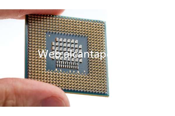
マイクロトレースPCBとは?
マイクロトレースPCBは優れた高精度です, 現代のエレクトロニクス産業で重要な役割を果たす高密度プリント基板. その製造プロセスでは、高度なマイクロトラッキング技術を使用して、回路トラッキングのサイズと間隔をミクロンレベルまで拡大しています。, 電子システムのパフォーマンスを強力にサポート.
従来のプリント基板製造は、多くの場合、プロセス技術と装置の精度によって制限されます。, 一方、Microtrace PCB は、ファイン トラッキング テクノロジーの適用によりこれらの制限を克服します。. マイクロトラッキングテクノロジーは、高度なCADソフトウェアと製造プロセスを使用して、回路レイアウトの極めて正確な制御を実現します。, 回路トラッキングのサイズと間隔をミクロンレベルに達することが可能. この精度の向上により、回路の安定性と信頼性が向上するだけではありません。, さまざまな複雑な電子システムの信号の完全性と電気的性能に対する高い要件も満たします。.
マイクロトレース プリント基板 複数のレベルで利点を提供する, そのうちの 1 つは優れたシグナル インテグリティです. マイクロトラッキング技術の応用により, Microtrace PCB の回路レイアウトはよりコンパクトになり、回路パスはより正確になります。, これにより、信号伝送中の損失と干渉が軽減されます。. この優れた信号整合性により、電子システムの安定した動作が確実に保証されます。, 特に高周波および高速回路でのアプリケーションに最適.
これに加えて, マイクロトレース PCB は優れた電気的性能を提供します. マイクロトラッキング技術は回路トラッキングの精度を向上させるだけではありません, より高密度な回路レイアウトも可能になります, 電子システムが同じサイズ内により多くの機能モジュールを統合できるようにする, システム全体のパフォーマンスの向上. 同時に, Microtrace PCB は多層設計をサポートします, より複雑な回路機能を実現し、さまざまなアプリケーションシナリオのニーズを満たすことができます.
総括する, マイクロトレースPCB, 高精度として, 高密度印刷回路基板, 現代の電子システムの設計と製造において重要な役割を果たします. 優れた信号整合性と電気的性能, 多層設計の柔軟性だけでなく, 電子システムの革新と発展の重要な原動力となる. テクノロジーの継続的な進歩とアプリケーションシナリオの継続的な拡大により、, マイクロトレース PCB は今後も重要な役割を果たし、エレクトロニクス産業の発展に新たな活力と力を注入していきます。.
マイクロトレース PCB 設計リファレンス ガイド.
マイクロトレース PCB の設計は、高性能電子デバイスを実現するための重要なステップの 1 つです. 設計プロセス中, 多くの要素を考慮する必要がある, 回路レイアウトも含めて, シグナルインテグリティ, 熱管理, 等, 最終製品の安定性と信頼性を確保するため. 以下は、Microtrace PCB 設計のリファレンス ガイドです。:
デザイン企画
設計を始める前に, まず回路の全体的な要件と機能を明確にする必要があります. 製品のアプリケーション シナリオとパフォーマンス要件を考慮する, 必要な回路の機能と特性を決定する.
概略設計
CADソフトを使って回路図を描きます。. 概略図では, 設計の正確性と完全性を確保するために、各コンポーネントの接続関係と機能が明確にマークされています。.
コンポーネントの選択
設計要件に従って適切なコンポーネントを選択します, チップを含む, コンデンサ, 抵抗器, 等. パフォーマンスなどの要素を考慮する, 信頼性, 最適なコンポーネントを選択するためのコスト.
レイアウトの最適化
さまざまなコンポーネントを PCB ボード上に合理的に配置します, 電気的性能などの要素を考慮して, シグナルインテグリティ, および熱管理. 信号線の長さとクロスオーバーを最小限に抑え、クロストークとノイズを低減します。.
ケーブル設計
コンポーネントのピンを接続して、スムーズで安定した信号伝送を確保します。. 信号損失と遅延を減らすために最適な配線方法を使用します。, 回路の性能と信頼性を向上させます.
電源設計
各コンポーネントの電源ニーズを確保するために、安定した信頼性の高い電源システムを設計します。. 電圧などの要因を考慮する, 現在, 適切な電源ソリューションとコンポーネントを選択するための電源.
熱管理
コンポーネントの過熱が性能と信頼性に影響を与えるのを防ぐために、PCB 設計における熱分布と放熱方法を考慮します。. ラジエーターと放熱経路を合理的に設計し、安定した回路動作を確保します.
チェックして検証する
デザインルールチェックの実施 (コンゴ民主共和国) および電気ルールのチェック (ERC) 正しい設計を保証するために. シミュレーションとテストを通じて, 回路の性能と信頼性が検証されています, 問題はタイムリーに発見され、解決されます.
上記は、Microtrace PCB 設計のリファレンス ガイドです。. 設計作業をより適切に実行し、高性能電子デバイスの開発と応用を成功させるのに役立つことを願っています。.
Microtrace PCB に使用されている材料?
Microtrace PCB の製造プロセスは、ボードの最高の品質とパフォーマンスを保証するために慎重に設計され、厳密に管理される非常に洗練されたプロセスです。. 以下は、Microtrace PCB 製造プロセスの詳細な手順です。:
マイクロトラッキング設計
マイクロトレース PCB の製造プロセスはマイクロトレース設計から始まります. このステップでは高度な CAD を使用します (コンピューター支援設計) ソフトウェア, 顧客のニーズと回路設計要件に基づいて、エンジニアがミクロンレベルの回路レイアウト設計を実行します。. CADソフトウェアを通じて, 回路基板上の各コンポーネントの位置と接続方法を正確に計画して、回路レイアウトが合理的で安定していることを保証できます。. この設計段階では、回路接続の機能だけを考慮するだけではありません。, ただし、回路基板の放熱やEMIなどの要因も考慮されます。 (電磁干渉) 最終製品の安定性と信頼性を確保するため.
高精度な印刷
次は高精度印刷の段階です. ファイントレース設計完了後, エンジニアは印刷技術を使用して、設計された回路パターンを基板上に正確に印刷します。. このプロセスでは、回路パターンの正確さと鮮明さを確保するために、高精度の印刷装置と正確なプロセス制御の使用が必要です。. 印刷完了後, 正確な回路レイアウトが基板上に表示されます, 処理の次のステップのための信頼できる基盤を提供する.
マイクロトラッキング処理
マイクロトレース処理は、マイクロトレース PCB 製造プロセスの重要なステップの 1 つです。. 回路パターン印刷完了後, 信号伝送の安定性と信頼性を確保するために、回路を正確に処理および追跡するには微細加工が必要です. このプロセスでは通常、高精度の切断および穴あけ装置を使用して、回路を正確に機械加工および穴あけします。, 各回路接続ポイントで最高の品質と精度を確保. マイクロトラッキング処理の精度と安定性は、最終製品の性能と信頼性に直接影響します。, したがって、製造プロセス全体で重要な役割を果たします.
品質検査
最後の重要なステップは品質検査です. マイクロトレース基板の製造完了後, 各回路基板が設計要件と基準を満たしていることを確認するには、厳格な品質検査が必要です。. 品質検査には外観検査も含まれます, 電気性能試験, 製品の安定性と信頼性が顧客の要件を満たしていることを確認するための追跡精度テストおよびその他の側面. 厳格な品質検査を通じてのみ、Microtrace PCB はさまざまな応用分野で最高の性能と効果を発揮することが保証されます。.
総括する, Microtrace PCB の製造プロセスは慎重に設計され、厳密に管理されています. マイクロトラッキング設計から高精度印刷まで, マイクロトラッキング処理から品質検査まで, 各ステップは細部に注意を払います, 最終製品の品質と性能を最高の状態に確実に到達させる. マイクロトレース PCB は、その優れた技術と信頼できる品質により、さまざまな高性能電子デバイスの最初の選択肢の 1 つとなっています。.
マイクロトレースPCBのサイズはどれくらいですか?
マイクロトレース PCB のサイズはアプリケーションと設計のニーズによって異なります, ただし、柔軟性とカスタマイズ性により、かなりの範囲のサイズに対応できます。. 通常, マイクロトレース PCB は、さまざまな電子デバイスの要件を満たすために、マイクロから大型までのさまざまなサイズで実装できます。.
マイクロデバイス用, マイクロトレース PCB は非常に小さいサイズに製造可能, それ以下でも 1 平方センチメートル. このマイクロサイズの Microtrace PCB は、ポータブル電子機器で一般的に使用されています, スマートウォッチなどの, ヘッドフォン, ポータブル医療監視機器, 等. サイズが小さいため、持ち運びに便利で快適な製品です。.
大型設備用, マイクロトレースPCBもニーズを満たすことができます. 例えば, 通信基地局や産業用制御システムなどの分野で, マイクロトレース PCB は、機器の安定性と信頼性を確保するために複雑な回路やコンポーネントを収容するために、より大きなサイズが必要になる場合があります。. このような場合には, マイクロトレース PCB の寸法は数十平方センチメートル、さらには数百平方センチメートルに達する場合もあります.
加えて, マイクロトレース基板も柔軟な形状設計が可能, 円形などの, 楕円形, 特殊な形状の, 等, スペースの制約や特定の機器の機能要件に適応するため. この柔軟性により、Microtrace PCB はさまざまなアプリケーションに最適です, 小型携帯機器でも大型産業機器でも.
全体として, Microtrace PCB には幅広いサイズがあり、特定のニーズに応じてカスタム設計できます, さまざまな電子機器の革新と開発を強力にサポートします. その柔軟性, 信頼性と高性能特性により、エレクトロニクス産業にとって不可欠かつ重要な部分となっています。, 将来の技術進歩に新たな活力を注入する.
マイクロトレース PCB の製造プロセス.
Microtrace PCB の製造プロセスは慎重に設計され、厳密に管理されています, マイクロトレース設計などの重要なステップを含む, 高精度印刷, マイクロトレース処理, そして品質検査.
初めに, マイクロトレース基板の製造工程で, マイクロトレース設計は重要なステップです. 高度なCADソフトウェアの助けを借りて, エンジニアはマイクロトレース設計を実行し、回路のレイアウトを正確に計画できます。. これには、各コンポーネントの位置の決定が含まれます。, ワイヤーの方向, 回路のレイアウトが合理的で安定していることを保証するための回路の接続方法と, 信号干渉と電力消費を最小限に抑える.
第二に, 高精度印刷は、Microtrace PCB 製造プロセスにおけるもう 1 つの重要なリンクです. 高度な印刷技術を使用, ファイントラッキングで設計された回路パターンを基板上に正確に印刷. これには、印刷の品質と精度を確保するための高度な機器と優れた技術が必要です。, これにより、その後の加工と組み立てのための強固な基盤を築きます。.
次, マイクロトレース処理は、マイクロトレース PCB 製造プロセスの重要なステップの 1 つです。. 微細加工技術による, 基板上に印刷された回路は正確に処理され、追跡されます。. これには、回路の精度と安定性を確保するために、レーザーや化学エッチングなどの技術を使用して余分なワイヤや金属層を正確に除去することが含まれます。. このステップの鍵は、信号伝送の安定性と信頼性を確保することです。, これにより、Microtrace PCB のパフォーマンスと信頼性が向上します。.
ついに, 品質検査は、Microtrace PCB 製造プロセスの重要な部分です. 厳しい品質検査を経て、, すべての Microtrace PCB が設計要件と規格を満たしていることを保証します. これには、回路の接続性を包括的に検査および評価するための高度なテスト機器とテクノロジーの使用が含まれます。, 連続, そして見た目のクオリティ. 厳格な品質検査を通じてのみ、Microtrace PCB の品質と信頼性が保証され、顧客のニーズと期待に応えることができます。.
総括する, Microtrace PCB の製造プロセスは慎重に設計され、厳密に管理されています, そしてすべてのステップが重要です. 緻密な設計によってのみ, 高品質の印刷, 精密な加工と厳しい品質検査により、高性能電子機器の要求を満たすマイクロトレース基板製品を生産できます。.
マイクロトレースPCBの応用分野.
マイクロトレース基板は、その高精度・高性能により、さまざまな分野の高性能電子機器で重要な役割を果たしています。. 以下は、さまざまな分野における Microtrace PCB の幅広い用途です。:
通信デバイス
マイクロトレースPCBは通信機器に広く使用されています, 基地局など, 通信ネットワーク機器, 等. これらのデバイスで, 高密度レイアウトと高周波信号伝送を実現するMicrotrace PCB, 通信機器の安定性と信頼性の確保.
医療機器
医療業界では、電子機器の安定性と精度に対して非常に高い要件が求められます。, Microtrace PCB はこれらのニーズを満たすことができます. さまざまな医療監視機器に使用されています, 診断装置, 等. 医療機器の精度と信頼性を確保するために.
航空宇宙
航空宇宙分野では、電子機器に対する非常に厳しい要件が求められます。, 極限環境における安定性と信頼性が求められる. マイクロトレース PCB はアビオニクス機器で広く使用されています, 衛星通信設備, 等. 極端な条件下でもこれらの機器が正常に動作することを保証するため.
自動化産業
産業オートメーションの分野では、高性能の制御システムとロボットが必要です, Microtrace PCB は高精度の信号伝送と安定した回路レイアウトを提供し、産業機器の精度と安定性を保証します。.
家電
家電の分野で, マイクロトレースPCBも重要な役割を果たします. スマートフォンやタブレットなどの家電製品には、高密度かつ高性能の回路基板が必要です, Microtrace PCB はこれらの要件を満たし、家庭用電子製品に安定した効率的なパフォーマンス サポートを提供します。.
総括する, マイクロトレースPCBは、さまざまな分野の高性能電子機器に広く使用されています, これらの機器の性能向上と革新のための重要なサポートを提供します, あらゆる分野の発展と進歩を促進する.
マイクロトレースPCBの利点は何ですか?
マイクロトレース PCB は、その独自の技術的利点と優れた性能により、電子機器製造の分野で非常に支持されています。. その利点は次のとおりです:
高精度のトラッキング
Microtrace PCB は、高度なマイクロトレーシング技術を使用して、回路のトラッキング ラインが高度な精度と安定性を備えていることを保証します。. 精密な設計と加工により、, マイクロトラッキング技術によりミクロンレベルの回路トラッキングを実現, 信号伝送の信頼性と安定性を向上. この高精度の追跡により、作業中の電子機器の効率と信頼性が保証されます。, ユーザーに優れたエクスペリエンスを提供する.
高密度レイアウト
Microtrace PCB は高密度レイアウトの機能を備えています, 限られたスペースでより多くの機能とコンポーネントの配置を実現できます. 高密度レイアウトにより電子機器の小型化・軽量化を実現, 製品の性能と機能を向上させながら. 通信機器であっても, 医療機器または産業用制御システム, マイクロトレース PCB は、その独自の利点を発揮して、より効率的な設計と生産を実現できます。.
優れた電気的性能
マイクロトレースPCBは優れた電気特性を持っています, 信号損失が少ないなど, 低騒音, 等. この優れた電気的性能により、Microtrace PCB は高性能電子機器の回路安定性と伝送品質要件を満たすことができます。, 製品の全体的なパフォーマンスレベルの向上. データ通信中かどうか, 信号処理または消費電力制御, Microtrace PCB はその独自の利点を最大限に発揮し、安定した信頼性の高いサービスをユーザーに提供します。.
多層設計
Microtrace PCB は多層設計をサポートします, より複雑な回路機能とレイアウトを可能にする. 多層設計による, 電子機器の性能や機能が向上するだけではなく、, だけでなく、より高いレベルの統合と最適化も達成できます。. 多層設計により、Microtrace PCB は幅広いアプリケーション シナリオに適しています。, さまざまな業界や分野のニーズに応えます, より多様な選択肢をユーザーに提供します.
カスタマイズされたサービス
Microtrace PCB はカスタマイズされたサービスを提供します, 顧客のニーズに応じたパーソナライズされた設計と製造. 回路レイアウトの点でも, 材料の選択またはプロセスの流れ, マイクロトレースPCBは顧客に応じて柔軟に調整可能’ さまざまな業界やアプリケーションのニーズを満たすための特定の要件. カスタマイズされたサービスにより、Microtrace PCB は顧客と緊密に連携して製品のイノベーションと開発を共同で促進し、より競争力のあるソリューションを市場に提供できるようになります。.
総括する, マイクロトレース PCB は、高精度のトラッキングなどの利点により、電子機器製造における最初の選択肢となっています。, 高密度レイアウト, 優れた電気性能, 多層設計とカスタマイズされたサービス, 顧客にあらゆるソリューションを提供する. そしてサポート.
よくある質問
マイクロトレース基板はどのような業界・分野に適していますか?
マイクロトレースPCBは、さまざまな分野の高性能電子機器に広く使用されています, 通信を含むがこれに限定されない, 医学, 航空宇宙, 産業オートメーションおよび家庭用電化製品.
マイクロトレース PCB の品質を保証する方法?
Microtrace PCB の製造プロセスでは、厳格な品質管理とテストが行われます。, マイクロトレース設計を含む, 高精度印刷, マイクロトレース処理, 各 PCB が設計要件と基準を満たしていることを確認するための品質検査.
マイクロトレース基板の生産サイクルはどのくらいですか?
マイクロトレース PCB の生産リードタイムは複雑さと量によって異なり、通常は数日から数週間の範囲です。. しかし、従来のPCBと比較すると、, 精密な製造プロセスにより、多少長くなる場合があります.
Microtrace PCB はカスタマイズされたサービスをサポートしていますか?
はい, Microtrace PCB はカスタマイズされたサービスを提供します, 顧客のニーズに応じたパーソナライズされた設計と製造, さまざまな業界や用途のニーズに対応, お客様に最適なソリューションを提供します.