株式会社")
とは何ですか 最小パッド クリアランス?
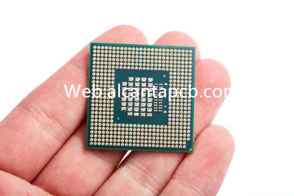
最小パッドクリアランス プリント基板 メーカー. マイクロトレースPCB, 非常に狭い間隔でのパッドからパッド、またはトレースからトレース , 極薄仕上げ基板厚さの PCB ベンダー. リジッドBT材料を使用してこのタイプのPCBを作成しました, 高速・高周波材料, または他のタイプの材料. これらのタイプの PCB を製造できます 2 レイヤーに 30 レイヤー.
最小パッドクリアランスは PCB の設計と製造における重要な概念です. はんだパッドの端間の最小許容距離を指します。 (またはパッド) および隣接する銅配線またはその他のフィーチャ. プリント基板上, パッドは通常、電子コンポーネントを接続するために使用されます, 一方、銅線は電流または信号を運ぶために使用されます. 最小パッドクリアランスを適切に設定することは、回路基板の電気的絶縁を確保し、短絡を回避するための重要な要素の 1 つです。.
PCB の設計および製造中, 各パッドには、隣接する銅配線またはフィーチャから良好に絶縁するために十分なクリアランスが必要です. パッド間の距離が狭すぎる場合, 電気ショートが発生し、回路基板や関連する電子部品が損傷する可能性があります。. したがって, 最小パッドクリアランスが仕様に準拠していることを確認することは、PCB の完全性と信頼性を確保するための重要な手順の 1 つです.
適切な最小パッドクリアランスを設定することにより, PCB がさまざまな環境条件で適切に機能することを保証できます。, 高温などの, 高湿度, または高振動環境. 加えて, 良好な最小パッドクリアランスは、PCB の耐干渉能力の向上にも役立ちます。, 信号干渉とクロストークを軽減する, これにより、回路のパフォーマンスと安定性が向上します。.
PCB設計段階中, エンジニアは、特定のアプリケーション要件と業界標準に基づいて、適切な最小パッドクリアランスを決定する必要があります。. 通常, 設計仕様では、PCB の信頼性とコンプライアンスを確保するための最小クリアランス要件を明確に指定します。. これらの仕様は PCB の目的によって異なる場合があります, 電気的特性, および環境条件.
ついに, 適切な最小パッドクリアランスを設定することは PCB のパフォーマンスと信頼性にとって重要であることに注意してください。, 大きいほど良いという意味ではありません. クリアランスが過剰になると、PCB のコストとサイズが増加し、回路密度と集積度が低下する可能性があります。. したがって, PCBを設計するとき, エンジニアは、よりコンパクトで効率的な設計を実現するために、最小ギャップ要件を満たしながら、パッド間のギャップを最小限に抑える必要があります。.
総括する, 最小パッドクリアランスは、PCB の設計と製造における重要なパラメータの 1 つです, それはパフォーマンスに直接影響します, 回路基板の信頼性とコスト. 最小パッドクリアランスを正しく設定することにより, さまざまな業界や分野のニーズを満たすさまざまなアプリケーションシナリオで PCB が安定して確実に動作できることを保証できます。.
なぜですか 最小パッドクリアランス PCB設計において重要?
PCB設計において, 最小パッドクリアランスの重要性は無視できません. この重要な設計指標はパフォーマンスに直接関係します。, 回路基板の安全性と耐用年数. 正しいクリアランス仕様を遵守しないと、さまざまな重大な問題が発生する可能性があります, 回路短絡や信号干渉を含む.
初め, 適切な最小パッドクリアランスを満たさないと、ショートが発生する可能性があります. プリント基板上, パッドと銅配線が直接接触しないように、それらの間に一定のギャップを維持する必要があります。. このギャップが不十分な場合, 短絡が発生し、電流が意図した経路をバイパスする可能性があります。, 回路中断を引き起こす, 過負荷, または電子部品の損傷.
第二に, 最小パッドクリアランスの仕様を満たさないと、信号干渉の問題が発生する可能性もあります. 回路基板上の信号線は異なる層間で交差することがよくあります. パッドが隣接する銅線またはフィーチャに近すぎる場合, 電磁波障害が発生します, 信号伝送の品質と安定性に影響を与える. これにより、データ転送エラーが発生する可能性があります, システムクラッシュ, またはパフォーマンスの低下.
最も重要なこと, 最小パッドクリアランスの仕様を遵守しないと、最終的には電子機器の故障につながります。. 家庭用電化製品でも産業用機器でも, それらはすべて、正常な動作を保証するために安定した信頼性の高い回路基板に依存しています。. PCB にクリアランスの問題がある場合, 機器の故障の原因となる可能性があります, 生産の中断につながる, 物的損害、さらには安全上のリスクも.
ボードのパフォーマンスと安全性に直接影響を与えるだけでなく、, 最小パッドクリアランスを遵守しないと、PCB の寿命が短くなる可能性もあります. 短絡や信号干渉などの問題により、電子部品が早期に損傷する可能性があります, それによりシステム全体の寿命が短くなります. さらに, 頻繁な故障や修理には PCB の交換が必要になる場合があります, これにより、メンテナンスコストが増加し、システムの信頼性が低下します.
要約すれば, PCB のパフォーマンスを確保するには、最小パッド クリアランス仕様を遵守することが重要です, 安全性, と信頼性. 適切な設計と仕様の厳密な実施を通じて, 潜在的な問題を防ぐことができます, 電子機器の適切な動作を保証し、その耐用年数を延ばします。.
最小パッドクリアランスの製造工程?
最小パッドクリアランスの処理は、PCB 製造プロセスにおける重要なステップです. メーカーは、PCB の品質と信頼性を確保するために、提供された設計仕様を厳密に遵守する必要があります。. 先進の機械と高度な技術を駆使して, 品質を損なうことなく最小パッドクリアランスの要件を満たすために一連の措置を講じています。.
初め, 基板の準備段階で, メーカーは基板の品質と表面の平坦性を注意深くチェックします. 最終製品の品質を確保するために、不良な基材は排除されます。. その後の製造プロセスをスムーズに進めるために、基板表面のコーティングと処理も設計仕様を満たす必要があります。.
次は銅パターン作成の段階です. この段階では, メーカーは化学エッチングまたは機械的除去を使用して、基板から不要な銅層を除去し、目的の回路パターンを形成します。. 最小限のパッドクリアランスを持つ PCB の製造において, メーカーはクリアランス要件を確実に満たすために、パッドからの距離を維持することに特別な注意を払う必要があります。.
エッチングプロセスは、PCB 製造における重要なステップの 1 つです. この過程で, メーカーは化学エッチングまたは機械的除去を使用して、基板から不要な銅層を除去し、目的の回路パターンを形成します。. メーカーは、最小パッドクリアランスへの影響を避けるために、エッチングプロセス中のエッチング時間と条件を正確に制御する必要があります。.
いよいよ掘削段階です. この段階では, メーカーは精密ドリルまたはレーザードリルを使用して、PCB に必要な穴を追加します。. 最小パッドクリアランスを扱う PCB で, メーカーは、設計仕様の要件を満たすためにドリル穴の位置とサイズが正確であることを確認する必要があります。.
要約すると, PCB 製造時に最小パッド クリアランスを処理するには、品質を損なうことなく設計仕様を確実に満たすための高度な機器と洗練された技術がメーカーに求められます。. この方法によってのみ、さまざまな応用分野のニーズを満たす高品質で信頼性の高い PCB を製造できます。.
最小パッドクリアランスに関するコストの考慮事項は何ですか??
最小パッドクリアランス仕様に準拠すると、PCB の設計と製造がある程度複雑になります。, しかし、すべてを考慮すると, 通常、メリットに比べてコストへの影響は最小限です. 実際には, ただし、PCB の製造には、より洗練されたプロセスとより高い品質管理基準が必要です。, こうした追加投資は長期的には価値がある.
初め, 最小パッドクリアランス仕様に準拠することで、PCB の電気的完全性が確保されます。. 適度な隙間を保つことで, 回路短絡や信号干渉などの問題を効果的に回避できます。, これにより、回路の安定性と信頼性が向上します。. これは、製造された PCB が故障する可能性が低いことを意味します。, 後の修理や交換のコストを削減する, ユーザーに長い耐用年数を提供します.
2番, クリアランス仕様を満たせば、PCB のパフォーマンスも向上します. 慎重に設計および製造された PCB を使用, 電子機器間の回路接続がより安定し、信号伝送がより確実になります。. これは、高いパフォーマンスと精度を必要とするアプリケーションにとって特に重要です。, 航空宇宙など, 医療機器, 等. これらの地域では, たとえ小さな欠陥や失敗であっても重大な結果をもたらす可能性があります, そのため、PCB の品質を確保することが重要です.
加えて, 最小パッドクリアランス仕様を遵守することで、生産プロセス全体の効率が向上します。. 仕様を確実に実装するには、設計および製造段階でより多くの時間とリソースが必要ですが、, この投資により、その後のエラー修正ややり直しが減り、時間とコストを節約できます。. 加えて, 標準化された設計仕様と製造プロセスを採用することで、人的エラーの発生を減らし、生産効率をさらに向上させることもできます。.
要約すれば, 最小パッドクリアランスの仕様に準拠すると、追加のコストと複雑さが追加される可能性があります, これらの追加投資をはるかに上回るメリットが得られます. PCB の電気的完全性を確保し、パフォーマンスと効率を向上させることによって, 仕様に準拠した PCB は、最終的にはより信頼性が高く安定した製品をユーザーに提供し、企業に長期的な経済的利益をもたらすことができます。. したがって, 最小パッドクリアランスの遵守への投資は、長期的には価値のある持続可能な投資です。.
最小パッドクリアランス PCB に使用されている材料?
最小パッドクリアランス PCB に使用される材料は、PCB の性能と信頼性に直接影響するため、非常に重要です。. プリント基板製造において, 高品質の材料の使用は、PCB が最小パッドクリアランス要件を確実に満たすための重要な要素の 1 つです。.
初め, 最小パッドクリアランス PCB で使用されるさまざまな材料を見てみましょう:
最小パッドクリアランス PCB の基板は通常 FR-4 材料で作られています, ガラス繊維強化エポキシ樹脂です. FR-4は耐熱性に優れた素材です。, 耐薬品性, そして機械的に強い, PCBの基板として最適です. 安定した誘電率と誘電損失を持っています, さまざまな環境条件下での PCB の安定性の確保.
銅は導電性に優れ、加工性が良いため、PCB ワイヤーには通常銅が使用されます。, PCBの複雑な回路の要件を満たすことができます. 銅導体は通常、化学エッチングや銅箔剥離などのプロセスを通じて、目的の線路の形状やサイズに加工されます。.
PCB内の異なる回路間の電気的絶縁と絶縁を確保するため, はんだマスクは絶縁層として使用されます. パッドは通常、PCB の表面を覆うポリマー フィルムです。. 絶縁性、耐食性に優れています, ワイヤ間の短絡や電気的干渉を効果的に防止できます。.
これらの材料は製造プロセスで重要な役割を果たすだけではありません, しかし、最終製品の性能と信頼性にとっても重要です. 精密な製造プロセスとの組み合わせ, 最小パッドクリアランス PCB の堅牢性と信頼性を保証します。.
PCB製造工程中, 適切な材料を選択し、正しく扱うことが重要です. メーカーは通常、顧客のニーズと設計要件に基づいて適切な材料を選択し、高度な製造技術を採用して PCB の品質と性能を確保します。. したがって, 高品質の材料と信頼できるメーカーを選択することは、最小パッドクリアランス PCB の製造を確実に成功させるための重要な要素の 1 つです。.
最小パッドクリアランス PCB 製造の主要なプレーヤーは誰ですか?
最小パッドクリアランス基板製造工程中, 主要なプレーヤーが重要な役割を果たし、協力して品質を保証します, PCB の信頼性と仕様への準拠. その中で, メーカーは中心的なプレーヤーの1つです.
PCB製造プロセスの主要プレーヤーの1つとして, メーカーは設計ファイルを実際のプリント回路基板に変換する責任があります。. 彼らは、高精度かつ効率的にPCB生産を完了するための高度な設備と技術を持っています。. メーカーは通常、顧客を理解するための豊富な経験と専門知識を持っています。’ ニーズを把握し、要件に基づいてカスタマイズされたソリューションを提供する.
メーカーは PCB 製造プロセス中にいくつかの重要な責任を負っています。. 初め, 顧客が提供した設計ファイルに基づいて PCB が正確に製造されていることを確認する必要があります。, 正しいレイアウトも含めて, ワイヤー接続, 最小パッドギャップ. 第二に, メーカーは業界の標準と仕様に厳密に準拠する必要があります, IPC-2221など, 等, 製造された PCB が品質要件を満たし、良好な電気特性と信頼性を備えていることを確認します。. 加えて, メーカーは生産プロセス中の品質管理も徹底する必要があります, 素材選びも含めて, 工程管理と最終検査, 各 PCB の品質が顧客の期待に応えられるようにするため.
最小パッドクリアランス基板製造工程中, 当社はメーカーの役割を果たします. 私たちは長年の経験と専門知識を基に、お客様に高品質な製品を提供することに尽力しています。, 信頼性が高くコスト効率の高いプリント基板ソリューション. 当社は、さまざまなPCB設計および仕様要件を満たす高度な製造設備と技術を備えています。. 同時に, 私たちはお客様とのコミュニケーションと協力を大切にし、当社の生産がお客様のニーズを満たし、カスタマイズされたソリューションを提供できるようにします。.
最小パッドクリアランス基板製造の中核企業として, メーカーは PCB の品質と信頼性を確保する上で重要な役割を果たしています. 当社, メーカーとして, 当社は、お客様の変化するニーズや課題に対応するために、高品質のプリント基板製品とサービスを提供できるよう引き続き努力してまいります。. 当社は、製造能力とサービスレベルを継続的に向上させるために資源とエネルギーを投資し続けます。, お客様と協力してより良い未来を創造します.
とは何ですか 5 優れた顧客サービスの資質?
優れた顧客サービスはビジネスの成功の重要な要素です. 顧客のニーズを満たすだけではない, それは長期的な関係を構築し維持するための基礎です. 優れた顧客サービスの 5 つの品質:
迅速な応答: 優れたカスタマーサービスチームは、顧客からの問い合わせに迅速かつ迅速に対応できる必要があります。, 質問や苦情. 電話かどうか, 電子メールまたはオンラインチャット, タイムリーなフィードバックにより、顧客は大切にされていると感じることができます, 彼らの信頼と満足度を高める.
専門知識: 製品やサービスを理解するための専門知識が、優れた顧客サービスを提供する鍵となります. 顧客は多くの場合、意思決定や問題解決に役立つ正確かつ詳細な情報を求めています。. 豊富な知識ベースを備えたカスタマーサービスチームは、顧客のニーズをより適切に満たし、ブランドの信頼性を高めることができます.
共感: 優れた顧客サービス担当者は、顧客の問題点とニーズを理解し、共感を示すことができなければなりません. 顧客が問題や困難に直面したときに、話を聞き、理解と共感を示すことで、顧客は大切にされている、大切にされていると感じることができます。, これにより、ブランドに対する顧客ロイヤルティが強化されます.
適応性のある: すべての顧客には独自のニーズと好みがあります, したがって、優れた顧客サービスチームは適応できるはずです. 顧客が最高のエクスペリエンスとサービスを受けられるようにするために、顧客のニーズに基づいて戦略とソリューションを適応できる必要があります。.
明確なコミュニケーション: クリア, 効果的なコミュニケーションは優れた顧客サービスの中核です. 顧客は、問題を理解して解決するプロセスを明確に理解する必要があります, そして、コミュニケーションプロセス全体を通じて適切なフィードバックを受け取る必要があります。. 明確なコミュニケーションを通じて, 顧客はサービスとソリューションをより深く理解できるようになります, 満足度を高め、ブランドとの関係を強化する.
全体, 優れた顧客サービスとは、単に電話に応答したり問題を解決したりすることだけではありません, 良好な関係を築き、ブランド価値を高める鍵です. 素早い対応などの属性により, 専門知識, 共感, 柔軟性と明確なコミュニケーション, 企業は顧客に優れたサービス体験を提供できる, 良いブランドイメージを確立する, 顧客ロイヤルティと評判を獲得します.
よくある質問
最小パッドクリアランスは PCB の性能と信頼性にどのように影響しますか?
最小パッドクリアランスは PCB の性能と信頼性に直接影響します. 指定されたクリアランス要件を遵守しないと、短絡が発生する可能性があります, 電子機器の機能を無効にする. 加えて, 不適切なギャップは信号干渉を引き起こす可能性があります, デバイスの安定性とデータ送信の精度に影響を与える.
PCB 設計が最小パッドクリアランスに準拠していることを確認するにはどうすればよいですか?
PCB 設計が最小パッドクリアランスに準拠していることを確認するには, まず適切な PCB 設計ソフトウェアを選択し、ギャップの仕様を理解する必要があります。. 設計プロセス中, コンポーネントの配置と配線に細心の注意を払う, デザインルールチェックツールを使用して、クリアランスが要件を満たしていることを確認します. タイムリーに設計を修正して、PCB 製造前に必要なクリアランス要件が確実に達成されるようにします。.
プリント基板製造において, 最小パッドクリアランスに特に注意を払う必要があるのはどのような場合ですか?
PCB設計の初期段階では、最小パッドクリアランスに特別な注意を払うことが重要です. 設計仕様と製造要件を決定する際には、最小パッドクリアランスの影響を考慮する必要があります。. さらに, 配置配線プロセス中, 最小クリアランス要件を常に念頭に置き、設計と製造の間のシームレスな移行を保証します。.
PCB 設計で最小パッド クリアランス違反を見つけた場合はどうすればよいですか?
PCB設計プロセス中に最小パッドクリアランス違反が発見された場合, それらを修正するために直ちに措置を講じる必要があります. コンポーネントのレイアウトを調整してクリアランス不足を解決する, ルート変更, またはデザインルールを変更する. 設計エラーを迅速に検査して修正することで、製造段階での重大な問題を回避し、最終製品の品質と信頼性を確保できます。.
PCB製造における最小パッドクリアランスに加えて, 他に考慮すべき重要な要素はありますか?
最小パッドクリアランスに加えて, PCB の設計および製造プロセス中に考慮する必要がある重要な要素は他にもたくさんあります。. これには回路レイアウトも含まれます, シグナルインテグリティ, 材料の選択, 環境条件とテスト要件, 等. これらの要素を考慮に入れることで、高性能の設計が保証されます。, 高信頼性PCB.