CO.,LTD")
FC-BGA multichip Substrati del pacchetto Produttore. Siamo un produttore leader di substrati per pacchetti FC-BGA multi-chip, specializzato in alte prestazioni, soluzioni affidabili per l'elettronica moderna. I nostri processi di produzione avanzati e la tecnologia all'avanguardia garantiscono una qualità superiore, sostenere le crescenti esigenze di alta densità, Applicazioni ad alta velocità nel calcolo, telecomunicazioni, ed elettronica di consumo.
Matrice di griglie multi-chip Flip Chip Ball (FC-BGA) pacchetto substrati sono componenti integrali dell'elettronica avanzata, fornendo una piattaforma per il montaggio e l'interconnessione di più chip semiconduttori all'interno di un unico pacchetto. Questi substrati sono progettati per supportare applicazioni di calcolo e comunicazione ad alte prestazioni, dove densa integrazione, trasmissione del segnale ad alta velocità, e una solida gestione termica sono essenziali. Questo articolo esplora le proprietà, struttura, processo di produzione, applicazioni, e vantaggi dei substrati del pacchetto FC-BGA multichip.
Cos'è un substrato del pacchetto FC-BGA multi-chip?
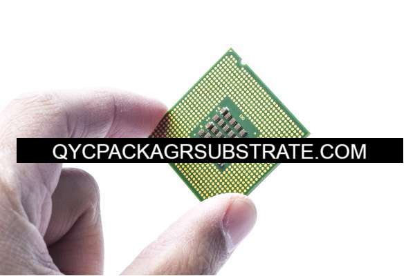
Una matrice di griglie multi-chip Flip Chip Ball (FC-BGA) il substrato del pacchetto è un sofisticato circuito stampato (PCB) che funge da base per il montaggio di più chip semiconduttori utilizzando la tecnologia flip-chip. L'approccio flip-chip prevede il fissaggio dei dischetti dei semiconduttori a faccia in giù sul substrato, consentendo collegamenti elettrici diretti tramite dossi di saldatura. Questo metodo riduce la lunghezza del percorso del segnale, migliora le prestazioni elettriche, e migliora la dissipazione del calore.
Il substrato FC-BGA incorpora una matrice di griglie di sfere (BGA) di sfere di saldatura sul lato inferiore, che facilita il montaggio superficiale su un circuito stampato (PCB). Questa configurazione consente interconnessioni ad alta densità, rendendolo adatto per applicazioni che richiedono notevole potenza di calcolo e trasmissione dati ad alta velocità.
Struttura dei substrati del pacchetto FC-BGA multichip
La struttura dei substrati del pacchetto Multi-Chip FC-BGA è complessa e multistrato, progettato per soddisfare i complessi requisiti delle applicazioni elettroniche ad alte prestazioni. Gli elementi strutturali chiave includono:
Lo strato centrale fornisce stabilità meccanica e costituisce la base strutturale primaria del substrato. In genere è realizzato con materiali come resina epossidica rinforzata con fibra di vetro o ceramica ad alte prestazioni, garantendo robustezza e stabilità dimensionale.
Si tratta di strati aggiuntivi aggiunti sopra lo strato centrale per aumentare la densità del cablaggio e consentire un instradamento complesso. Sono costruiti utilizzando materiali con elevate prestazioni termiche ed elettriche per supportare la trasmissione del segnale ad alta velocità e la distribuzione dell'energia.
La maschera di saldatura è uno strato protettivo che copre la superficie del substrato, prevenendo ponti di saldatura e proteggendo i circuiti sottostanti. Finiture superficiali, come l'oro ad immersione in nichel chimico (ESSERE D'ACCORDO) o conservante organico di saldabilità (OSP), vengono applicati ai cuscinetti di contatto per garantire connessioni di saldatura affidabili.
Questi includono i via, microvie, e fori passanti che forniscono collegamenti elettrici tra diversi strati del substrato. Tecniche avanzate come la perforazione laser e la laminazione sequenziale vengono utilizzate per creare queste strutture con elevata precisione.
Alcuni substrati FC-BGA multichip incorporano componenti passivi incorporati, come resistori e condensatori, all'interno degli strati del substrato. Questa integrazione aiuta a ridurre le dimensioni complessive del pacchetto e migliora le prestazioni elettriche riducendo al minimo gli effetti parassiti.
Materiali utilizzati nei substrati del pacchetto FC-BGA multichip
I materiali utilizzati nella costruzione dei substrati del contenitore multi-chip FC-BGA sono selezionati per la loro eccellente termica, elettrico, e proprietà meccaniche. I materiali chiave includono:
Resine epossidiche ad alte prestazioni, spesso rinforzato con fibra di vetro, vengono utilizzati per gli strati centrali e di ricostruzione. Questi materiali forniscono la resistenza meccanica e la stabilità termica necessarie per un funzionamento affidabile.
Il rame è ampiamente utilizzato per gli strati conduttivi e le interconnessioni grazie alla sua eccellente conduttività elettrica. Sottili lamine di rame vengono laminate sugli strati del substrato e modellate per formare le tracce del circuito.
Materiali dielettrici, come poliimmide o polimero cristallino liquido (LCP), vengono utilizzati come strati isolanti tra le tracce conduttrici. Questi materiali hanno costanti dielettriche e tangenti di perdita basse, garantendo un'attenuazione minima del segnale e prestazioni ad alta velocità.
Per migliorare la gestione termica, materiali avanzati per l'interfaccia termica (TIM) vengono utilizzati. Questi materiali facilitano un efficiente trasferimento di calore dalle matrici dei semiconduttori al substrato, prevenendo il surriscaldamento e garantendo un funzionamento affidabile.
Finiture superficiali come ENIG o OSP vengono applicate ai cuscinetti di contatto per migliorare la saldabilità e proteggere dall'ossidazione. Queste finiture garantiscono giunti di saldatura affidabili e durata a lungo termine del substrato.
Il processo di produzione dei substrati del pacchetto FC-BGA multichip
Il processo di produzione dei substrati del pacchetto FC-BGA multichip prevede diverse fasi critiche, ciascuno essenziale per ottenere l'elevata precisione e le prestazioni richieste per le applicazioni elettroniche avanzate. Il processo include:
Materie prime di alta qualità, comprese le resine epossidiche, lamine di rame, e pellicole dielettriche, sono preparati e ispezionati per garantire che soddisfino le specifiche richieste.
Lo strato centrale e gli strati successivi vengono laminati insieme utilizzando calore e pressione per formare un substrato unificato. Questo passaggio prevede un allineamento e un controllo precisi per garantire che gli strati siano adeguatamente incollati e registrati.
Vie e fori passanti vengono praticati nel substrato per creare interconnessioni elettriche tra gli strati. Questi fori vengono quindi placcati con rame per stabilire percorsi conduttivi.
Gli schemi dei circuiti sono realizzati mediante processi fotolitografici. Ciò comporta l'applicazione di una pellicola fotosensibile (fotoresist) alla superficie del rame, esponendolo ai raggi ultravioletti (UV) luce attraverso una maschera, e sviluppare le aree esposte per rivelare gli schemi circuitali desiderati. Il substrato viene quindi inciso per rimuovere il rame indesiderato, lasciando dietro di sé le tracce del circuito.
Una maschera di saldatura viene applicata al substrato per proteggere i circuiti ed evitare ponti di saldatura durante l'assemblaggio. La maschera di saldatura viene generalmente applicata utilizzando tecniche di serigrafia o di imaging fotografico e quindi polimerizzata per indurirla.
Le finiture superficiali vengono applicate ai cuscinetti di contatto per migliorare la saldabilità e proteggere dall'ossidazione. Tecniche come ENIG o OSP vengono utilizzate per garantire giunti di saldatura affidabili e durata a lungo termine.
I substrati finali vengono sottoposti a controlli e test rigorosi per garantire che soddisfino tutti gli standard di prestazioni e affidabilità. Test elettrici, ispezione visiva, e ispezione ottica automatizzata (AOI) servono per individuare eventuali difetti o irregolarità.
Aree di applicazione dei substrati del package FC-BGA multichip
I substrati del pacchetto FC-BGA multichip sono utilizzati in un'ampia gamma di applicazioni in vari settori grazie alle loro capacità ad alte prestazioni. Le principali aree di applicazione includono:
Questi substrati sono utilizzati nei sistemi informatici ad alte prestazioni, come server e data center, dove sono essenziali una fitta integrazione e una trasmissione del segnale ad alta velocità. Supportano processori multi-core e moduli di memoria avanzati, consentendo un'elaborazione e un'archiviazione efficienti dei dati.
Nelle telecomunicazioni, I substrati FC-BGA multichip vengono utilizzati nelle apparecchiature dell'infrastruttura di rete, come i router, interruttori, e stazioni base. Le loro interconnessioni ad alta densità e le robuste capacità di gestione termica garantiscono prestazioni affidabili in ambienti di comunicazione esigenti.
I substrati FC-BGA multichip si trovano nell'elettronica di consumo, compresi gli smartphone, compresse, e console di gioco. Questi substrati consentono l'integrazione di più chip semiconduttori, fornendo funzionalità e prestazioni migliorate in fattori di forma compatti.
L'industria automobilistica utilizza substrati FC-BGA multichip in sistemi avanzati di assistenza alla guida (ADAS), sistemi di infotainment, e centraline controllo motore (ECU). Questi substrati forniscono le prestazioni e l'affidabilità necessarie per le applicazioni automobilistiche critiche.
Nel settore aerospaziale e della difesa, I substrati FC-BGA multichip sono utilizzati nell'avionica, sistemi radar, e apparecchiature di comunicazione satellitare. La loro capacità di resistere a condizioni ambientali difficili e di fornire una trasmissione dati ad alta velocità li rende ideali per queste applicazioni.
Vantaggi dei substrati del pacchetto FC-BGA multichip
I substrati dei pacchetti FC-BGA multichip offrono numerosi vantaggi che li rendono la scelta preferita per le applicazioni elettroniche ad alte prestazioni. Questi vantaggi includono:
I substrati FC-BGA multichip consentono l'integrazione di più chip semiconduttori all'interno di un unico pacchetto, ridurre le dimensioni e il peso complessivi dei dispositivi elettronici. Questa integrazione ad alta densità è essenziale per applicazioni compatte e portatili.
La tecnologia flip-chip e le strutture di interconnessione avanzate utilizzate nei substrati FC-BGA multi-chip garantiscono una perdita di segnale e interferenze minime. Ciò si traduce in prestazioni elettriche superiori e trasmissione dati ad alta velocità, fondamentale per i moderni sistemi elettronici.
I substrati FC-BGA multichip sono progettati per dissipare il calore in modo efficace, prevenire il surriscaldamento e garantire il funzionamento affidabile dei componenti elettronici. I materiali di interfaccia termica avanzati e i design termici ottimizzati migliorano la capacità del substrato di gestire il calore.
La struttura robusta e i materiali di alta qualità utilizzati nei substrati FC-BGA multichip garantiscono prestazioni affidabili in ambienti difficili. Questi substrati sono progettati per resistere ai cicli termici, sollecitazione meccanica, e condizioni difficili, rendendoli adatti ad applicazioni critiche.
Domande frequenti
Ciò che rende i substrati del pacchetto FC-BGA multichip adatti per applicazioni elettroniche ad alte prestazioni?
I substrati del pacchetto FC-BGA multichip sono ideali per applicazioni elettroniche ad alte prestazioni grazie alla loro integrazione ad alta densità, prestazioni elettriche migliorate, Efficiente gestione termica, e robuste proprietà meccaniche. Queste caratteristiche consentono un funzionamento affidabile ed efficiente in ambienti difficili.
I substrati del pacchetto FC-BGA multichip possono essere utilizzati in ambienti ad alta temperatura?
SÌ, I substrati del pacchetto FC-BGA multichip sono particolarmente adatti per ambienti ad alta temperatura. Le loro eccellenti capacità di gestione termica e la struttura robusta garantiscono prestazioni affidabili in condizioni di stress termico, rendendoli ideali per applicazioni quali l'elettronica automobilistica e i sistemi aerospaziali.
In che modo i substrati del pacchetto FC-BGA multichip garantiscono un'efficace gestione termica?
I substrati del pacchetto FC-BGA multichip garantiscono una gestione termica efficace attraverso materiali di interfaccia termica avanzati e design termici ottimizzati. Queste caratteristiche facilitano un'efficiente dissipazione del calore dai chip semiconduttori al substrato, prevenendo il surriscaldamento e garantendo un funzionamento affidabile.
Quali settori traggono maggiori vantaggi dall'utilizzo di substrati di pacchetti FC-BGA multi-chip?
I settori che traggono i maggiori vantaggi dall'utilizzo di substrati di pacchetti FC-BGA multichip includono l'elaborazione ad alte prestazioni, telecomunicazioni, elettronica di consumo, Elettronica automobilistica, e aerospaziale e difesa. Questi settori richiedono un’integrazione ad alta densità, prestazioni elettriche migliorate, ed efficiente gestione termica, forniti dai substrati FC-BGA multichip.