株式会社")
マルチチップFC-BGA パッケージ基板 メーカー。当社はマルチチップFC-BGAパッケージ基板の大手メーカーです。, 高性能に特化した, 最新のエレクトロニクス向けの信頼できるソリューション. 高度な製造プロセスと最先端のテクノロジーが優れた品質を保証します, 高密度化への要求の高まりをサポート, コンピューティングにおける高速アプリケーション, 電気通信, およびコンシューマーエレクトロニクス.
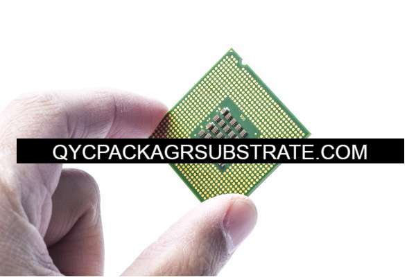
マルチチップ フリップチップ ボール グリッド アレイ (FC-BGA) パッケージ 基板 高度なエレクトロニクスに不可欠なコンポーネントです, 単一パッケージ内に複数の半導体チップを実装および相互接続するためのプラットフォームを提供します。. これらの基板は、高性能コンピューティングおよび通信アプリケーションをサポートするように設計されています。, ここで高密度の統合, 高速信号伝送, 堅牢な熱管理が不可欠です. この記事では、プロパティについて説明します, 構造, 製造工程, アプリケーション, マルチチップFC-BGAパッケージ基板のメリットとメリット.
マルチチップFC-BGAパッケージ基板とは?
マルチチップ フリップチップ ボール グリッド アレイ (FC-BGA) パッケージ基板は洗練されたプリント基板です (プリント基板) フリップチップ技術を使用して複数の半導体チップを実装するための基盤として機能します. フリップチップ手法では、半導体ダイを下向きに基板に取り付ける必要があります。, はんだバンプを介した直接電気接続が可能. この方法により信号経路長が短縮されます, 電気的性能を向上させます, 放熱性を向上させます.
FC-BGA基板にはボールグリッドアレイが組み込まれています (BGA) はんだボールの下側, プリント基板への表面実装が容易になります。 (プリント基板). この構成により、高密度の相互接続が可能になります, 大量の計算能力と高速データ伝送を必要とするアプリケーションに適しています。.
マルチチップFC-BGAパッケージ基板の構造
マルチチップFC-BGAパッケージ基板の構造は複雑かつ多層です, 高性能電子アプリケーションの複雑な要件に対応するように設計されています. 主要な構造要素には次のものがあります。:
コア層は機械的安定性を提供し、基板の主要な構造ベースを形成します。. 通常、ガラス繊維強化エポキシ樹脂や高性能セラミックなどの材料で作られています。, 堅牢性と寸法安定性を確保.
これらは、配線密度を高め、複雑な配線を可能にするためにコア層の上に追加される追加層です。. これらは、高速信号伝送と配電をサポートするために、高い熱的および電気的性能を備えた材料を使用して構築されています。.
ソルダーマスクは基板の表面を覆う保護層です, はんだブリッジを防止し、その下にある回路を保護します。. 表面仕上げ, 無電解ニッケル浸漬金など (同意する) または有機はんだ付け性保存剤 (OSP), 信頼性の高いはんだ接続を確保するために接触パッドに適用されます.
これらにはビアが含まれます, マイクロバイアス, 基板の異なる層間に電気接続を提供するスルーホール. レーザー穴あけや連続積層などの高度な技術を使用して、これらの構造を高精度で作成します。.
一部のマルチチップ FC-BGA 基板には、受動部品が組み込まれています, 抵抗器やコンデンサーなど, 基板層内で. この統合により、パッケージ全体のサイズが縮小され、寄生効果が最小限に抑えられることで電気的性能が向上します。.
マルチチップFC-BGAパッケージ基板に使用される材料
マルチチップ FC-BGA パッケージ基板の構築に使用される材料は、優れた熱特性を考慮して選択されています。, 電気, および機械的特性. 主な材料には以下が含まれます::
高性能エポキシ樹脂, 多くの場合グラスファイバーで強化されています, コア層とビルドアップ層に使用されます. これらの材料は、信頼性の高い動作に必要な機械的強度と熱安定性を提供します。.
銅はその優れた導電性により、導電層や配線に広く使用されています。. 薄い銅箔が基板層に積層され、パターン化されて回路トレースが形成されます。.
誘電体材料, ポリイミドや液晶ポリマーなど (LCP), 導電性トレース間の絶縁層として使用されます。. これらの材料は誘電率と損失正接が低いです, 最小限の信号減衰と高速パフォーマンスを保証します。.
熱管理を強化するには, 先進的なサーマルインターフェース材料 (ティム) 使用されています. これらの材料は、半導体ダイから基板への効率的な熱伝達を促進します。, 過熱を防止し、信頼性の高い動作を保証します.
ENIG や OSP などの表面仕上げがコンタクト パッドに適用され、はんだ付け性が向上し、酸化から保護されます。. これらの仕上げにより、信頼性の高いはんだ接合と基板の長期耐久性が保証されます。.
マルチチップFC-BGAパッケージ基板の製造プロセス
マルチチップ FC-BGA パッケージ基板の製造プロセスには、いくつかの重要なステップが含まれます, それぞれが高度な電子アプリケーションに必要な高精度と性能を実現するために不可欠です. プロセスには以下が含まれます:
高品質の原材料, エポキシ樹脂を含む, 銅箔, および誘電体膜, 要求された仕様を満たしていることを確認するために準備および検査されます。.
コア層とビルドアップ層を熱と圧力で貼り合わせて一体化した基板を形成します。. このステップには、層が適切に接着され、位置合わせされていることを確認するための正確な位置合わせと制御が含まれます。.
ビアとスルーホールが基板に開けられ、層間の電気的相互接続が作成されます。. これらの穴は銅でメッキされ、導電経路が確立されます。.
回路パターンはフォトリソグラフィープロセスを使用して作成されます. これには、感光性フィルムを塗布することが含まれます。 (フォトレジスト) 銅の表面に, 紫外線に当てると (紫外線) マスクを通した光, 露光領域を現像して、目的の回路パターンを明らかにします。. 次に、基板をエッチングして不要な銅を除去します。, 回路の痕跡を残す.
回路を保護し、組み立て中のはんだブリッジを防ぐために、はんだマスクが基板に適用されます。. はんだマスクは通常、スクリーン印刷またはフォトイメージング技術を使用して塗布され、その後硬化されて硬化されます。.
はんだ付け性を向上させ、酸化から保護するために、コンタクトパッドに表面仕上げが施されています。. ENIG や OSP などの技術を使用して、信頼性の高いはんだ接合と長期耐久性を確保します。.
最終的な基板は厳格な検査とテストを受け、すべての性能と信頼性の基準を満たしていることを確認します。. 電気試験, 目視検査, 自動光学検査 (あおい) 欠陥や異常を特定するために使用されます.
マルチチップFC-BGAパッケージ基板の応用分野
マルチチップ FC-BGA パッケージ基板は、その高性能機能により、さまざまな業界の幅広いアプリケーションで使用されています. 主な応用分野は次のとおりです。:
これらの基板は高性能コンピューティング システムで使用されます。, サーバーやデータセンターなど, 高密度な集積化と高速信号伝送が不可欠な場所. マルチコアプロセッサと高度なメモリモジュールをサポートしています, 効率的なデータ処理とストレージを可能にする.
通信で, マルチチップFC-BGA基板はネットワークインフラ機器に使用されています, ルーターなどの, スイッチ, と基地局. 高密度の相互接続と堅牢な熱管理機能により、要求の厳しい通信環境でも信頼性の高いパフォーマンスが保証されます。.
マルチチップ FC-BGA 基板は家庭用電化製品に使用されています, スマートフォンを含む, 錠剤, およびゲーム機. これらの基板により、複数の半導体チップの集積が可能になります。, コンパクトなフォームファクターで強化された機能とパフォーマンスを提供.
自動車業界は、高度な運転支援システムでマルチチップ FC-BGA 基板を使用しています (ADAS), インフォテイメント システム, およびエンジン制御ユニット (ECU). これらの基板は、重要な自動車用途に必要な性能と信頼性を提供します。.
航空宇宙と防御で, マルチチップ FC-BGA 基板はアビオニクスで使用されます, レーダーシステム, および衛星通信設備. 過酷な環境条件に耐え、高速データ伝送を実現できるため、これらのアプリケーションに最適です。.
マルチチップFC-BGAパッケージ基板のメリット
マルチチップ FC-BGA パッケージ基板には、高性能電子アプリケーションに最適な選択肢となるいくつかの利点があります。. これらの利点には以下が含まれます::
マルチチップ FC-BGA 基板により、単一パッケージ内に複数の半導体チップを統合できます。, 電子機器全体のサイズと重量を削減する. この高密度の統合は、コンパクトでポータブルなアプリケーションには不可欠です.
マルチチップ FC-BGA 基板で使用されるフリップチップ技術と高度な相互接続構造により、信号損失と干渉を最小限に抑えます。. これにより、優れた電気的性能と高速データ伝送が実現します。, 現代の電子システムにとって重要な要素.
マルチチップ FC-BGA 基板は、熱を効果的に放散するように設計されています, 過熱を防止し、電子部品の信頼性の高い動作を確保します。. 高度なサーマルインターフェース材料と最適化された熱設計により、基板の熱管理能力が強化されます。.
マルチチップ FC-BGA 基板に使用される堅牢な構造と高品質の素材により、要求の厳しい環境でも信頼性の高いパフォーマンスが保証されます。. これらの基板は熱サイクルに耐えるように設計されています, 機械的ストレス, そして過酷な条件, クリティカルなアプリケーションに適したものにする.
よくある質問
マルチチップ FC-BGA パッケージ基板が高性能電子アプリケーションに適している理由?
マルチチップ FC-BGA パッケージ基板は、高密度集積により高性能電子アプリケーションに最適です, 電気性能の向上, 効率的な熱管理, 堅牢な機械的特性. これらの特性により、要求の厳しい環境でも信頼性が高く効率的な運用が可能になります。.
マルチチップ FC-BGA パッケージ基板は高温環境でも使用できますか?
はい, マルチチップ FC-BGA パッケージ基板は高温環境に非常に適しています. 優れた熱管理機能と堅牢な構造により、熱ストレス下でも信頼性の高いパフォーマンスが保証されます。, 自動車エレクトロニクスや航空宇宙システムなどの用途に最適です。.
マルチチップ FC-BGA パッケージ基板はどのようにして効果的な熱管理を保証するのか?
マルチチップ FC-BGA パッケージ基板は、高度なサーマル インターフェイス材料と最適化された熱設計を通じて効果的な熱管理を保証します。. これらの機能により、半導体チップから基板への効率的な熱放散が促進されます。, 過熱を防止し、信頼性の高い動作を保証します.
マルチチップ FC-BGA パッケージ基板を使用することで最も恩恵を受けるのはどの業界ですか?
マルチチップ FC-BGA パッケージ基板の使用から最も恩恵を受ける業界には、ハイ パフォーマンス コンピューティングが含まれます, 電気通信, 家電, 自動車エレクトロニクス, 航空宇宙と防衛. これらの業界では高密度の統合が必要です, 電気性能の向上, 効率的な熱管理, マルチチップ FC-BGA 基板が提供するもの.