株式会社")
GPUパッケージ基板メーカー。GPUのリーディングカンパニーとして パッケージ基板 メーカー, 私たちは高性能を提供することに特化しています, 高度なグラフィックス処理装置のための信頼できるソリューション. 当社の最先端の設備と革新的なエンジニアリングにより、すべての製品で最高レベルの品質と精度が保証されます。. ゲームの厳しいニーズに応えます, AI, データセンター産業, 熱管理を強化する基板の提供, シグナルインテグリティ, そして全体的なパフォーマンス. コンピューティングの未来を推進する最先端の GPU パッケージング テクノロジーなら当社にお任せください。.
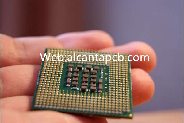
GPU (グラフィックスプロセッシングユニット) パッケージ基板は現代のコンピューティングに不可欠なコンポーネントです, GPU のさまざまな電子コンポーネントを取り付け、相互接続するための基礎的なプラットフォームを提供します。. これらの基板は、高性能グラフィックス処理に必要な高密度統合と効率的な熱管理をサポートするように設計されています。. GPUは幅広いアプリケーションでますます重要になる, ゲームやプロ仕様のグラフィックスから人工知能や科学技術コンピューティングまで, GPUパッケージ基板の役割はこれまで以上に重要になっています. この記事では、プロパティについて説明します, 構造, 材料, 製造工程, アプリケーション, とGPUパッケージ基板のメリット.
GPUパッケージ基板とは?
GPU パッケージ基板は、グラフィックス処理ユニットのコンポーネントを組み立て、相互接続するために使用されるベース素材の一種です。. シリコンチップとプリント基板の間の仲介者として機能します。 (プリント基板), 機械的サポートと電気的接続を提供する. GPU パッケージ基板は、最新の GPU に必要な高密度配線と複雑な相互接続に対応できるように設計されています。.
GPU パッケージ基板は通常、優れた電気絶縁性を備えた先進的な材料で作られています。, 熱伝導率, 機械的安定性. GPU のパッケージングに不可欠です, 繊細な半導体コンポーネントが確実に保護され、高性能条件下で効率的に動作できるようにします。.
GPUパッケージ基板の構造
GPUのパッケージ基板の構造は複雑かつ多層になっています, 高性能グラフィックス処理の厳しい要件を満たすように設計されています. 主要な構造要素には次のものがあります。:
コア層は基板の一次構造を形成します。, 機械的な安定性と剛性を提供します. 通常、ガラス繊維強化エポキシ樹脂やセラミックなどの材料で作られています。.
これらの層はコア層の上に追加され、配線密度を高め、複雑な回路パターンをサポートします。. ビルドアップ層は最先端の誘電体材料を使用して構築されており、最適な電気的性能を保証します.
導電層, 通常は銅で作られています, 基板上のさまざまなコンポーネントを相互接続する回路トレースを形成します。. これらの層はフォトリソグラフィープロセスを使用してパターン化され、正確で高密度の配線が作成されます。.
ビアは、基板の異なる層を接続する垂直相互接続です。. 高度な穴あけ技術を使用して作成されています, レーザー穴あけなど, 高い精度と信頼性を確保するために.
表面仕上げ, 無電解ニッケル浸漬金など (同意する) または有機はんだ付け性保存剤 (OSP), はんだ付け性を向上させ、酸化を防ぐためにコンタクトパッドに塗布されます。.
はんだマスクは、導電性トレースを環境による損傷から保護し、組み立て中のはんだブリッジを防ぐために適用されます。.
GPUパッケージ基板に使用される材料es
GPU パッケージ基板の材料の選択は、パフォーマンスと信頼性にとって重要です。. 主な材料には以下が含まれます::
エポキシ樹脂, 多くの場合グラスファイバーで強化されています, 一般的にコア層とビルドアップ層に使用されます. これらの材料は、優れた機械的強度と熱安定性を提供します。.
高機能セラミックス, アルミナ、窒化アルミニウムなど, 優れた熱伝導性と電気絶縁性を提供するために、一部の GPU パッケージ基板で使用されています。.
銅は優れた導電性を備えているため、導電層に広く使用されています。. 薄い銅箔が基板に積層され、パターン化されて回路トレースが形成されます。.
信号減衰を最小限に抑え、高周波性能を確保するために、低誘電率と低損失正接を備えた高度な誘電体材料が使用されています。.
ENIG および OSP は、はんだ付け性を向上させ、接触パッドを酸化や腐食から保護するために一般的に使用される表面仕上げです。.
GPUパッケージ基板の製造工程
GPU パッケージ基板の製造プロセスには、高品質とパフォーマンスを確保するために、正確に管理されたいくつかの手順が含まれます. 主な手順には以下が含まれます:
高品質の原材料, エポキシ樹脂を含む, 銅箔, および誘電体膜, 要求された仕様を満たしていることを確認するために準備および検査されます。.
コア層とビルドアップ層を熱と圧力で貼り合わせて一体化した基板を形成します。. このステップには、層が適切に接着されていることを確認するための正確な位置合わせと制御が含まれます。.
ビアとスルーホールが基板に開けられ、層間の電気的相互接続が作成されます。. これらの穴は銅でメッキされ、導電経路が確立されます。.
回路パターンはフォトリソグラフィープロセスを使用して作成されます. これには、感光性フィルムを塗布することが含まれます。 (フォトレジスト) 銅の表面に, 紫外線に当てると (紫外線) マスクを通した光, 露光領域を現像して、目的の回路パターンを明らかにします。. 次に、基板をエッチングして不要な銅を除去します。, 回路の痕跡を残す.
回路を保護し、組み立て中のはんだブリッジを防ぐために、はんだマスクが基板に適用されます。. はんだマスクは通常、スクリーン印刷またはフォトイメージング技術を使用して塗布され、その後硬化されて硬化されます。.
はんだ付け性を向上させ、酸化から保護するために、コンタクトパッドに表面仕上げが施されています。. ENIG や OSP などの技術を使用して、信頼性の高いはんだ接合と長期耐久性を確保します。.
最終的な基板は厳格な検査とテストを受け、すべての性能と信頼性の基準を満たしていることを確認します。. 電気試験, 目視検査, 自動光学検査 (あおい) 欠陥や異常を特定するために使用されます.
GPUパッケージ基板の応用分野
GPU パッケージ基板は、さまざまな業界の幅広い電子アプリケーションで使用されています. 主な応用分野は次のとおりです。:
GPU はゲーム コンソールで高解像度のグラフィックスをレンダリングするために不可欠です, パソコン, および仮想現実システム. GPU パッケージ基板は、これらの要求の厳しいアプリケーションに必要なパフォーマンスと信頼性を提供します。.
アニメなどの業界では, 映画制作, そしてグラフィックデザイン, GPU は、複雑なグラフィックスや視覚効果のレンダリングに使用されます. GPU パッケージ基板は、これらのプロフェッショナル アプリケーションの高性能要件をサポートします。.
GPU は、その並列処理能力により、AI および機械学習タスクにますます使用されています。. GPU パッケージ基板により、AI ワークロードに必要な高密度統合と効率的な熱管理が可能になります.
科学研究とシミュレーションにおいて, GPU は複雑な計算とデータ分析を高速化します. GPU パッケージ基板は、こうした一か八かのアプリケーションで信頼性の高いパフォーマンスを保証します.
GPUは先進運転支援システムに使用されています (ADAS) および自動運転技術. GPU パッケージ基板は、これらの車載アプリケーションに必要なパフォーマンスと耐久性を提供します。.
GPUパッケージ基板のメリット
GPU パッケージ基板には、現代のコンピューティング アプリケーションに不可欠ないくつかの利点があります。. これらの利点には以下が含まれます::
GPUパッケージ基板は電子部品の高密度集積をサポート, 複雑な機能の組み込みを可能にし、全体的なパフォーマンスを向上させます。.
GPU パッケージ基板に使用される先進的な素材と精密な製造プロセスにより、信号損失と干渉を最小限に抑えます。, 優れた電気的性能を実現.
GPU パッケージ基板は熱を効果的に放散するように設計されています, 過熱を防止し、GPU コンポーネントの信頼性の高い動作を確保します。.
GPU パッケージ基板に使用される堅牢な構造と高品質の素材により、要求の厳しい環境でも信頼性の高いパフォーマンスが保証されます。. これらの基板は熱サイクルに耐えるように設計されています, 機械的ストレス, そして過酷な条件.
よくある質問
GPU パッケージ基板がハイパフォーマンス コンピューティング アプリケーションに適している理由?
GPU パッケージ基板は、高密度に統合されているため、高性能コンピューティング アプリケーションに適しています。, 電気性能の向上, 効率的な熱管理, 堅牢な機械的特性. これらの特性により、要求の厳しい環境でも信頼性が高く効率的な運用が可能になります。.
GPUパッケージ基板は高温環境でも使用できますか?
はい, GPU パッケージ基板は高温環境に非常に適しています. 優れた熱管理機能と堅牢な構造により、熱ストレス下でも信頼性の高いパフォーマンスが保証されます。, ゲームやプロ仕様のグラフィックスなどのアプリケーションに最適です。.
GPU パッケージ基板はどのようにして効果的な熱管理を保証するのか?
GPU パッケージ基板は、高い熱伝導率と最適化された熱設計を備えた先進的な材料の使用により、効果的な熱管理を保証します。. これらの機能により、GPU コンポーネントから基板への効率的な熱放散が促進されます。, 過熱を防止し、信頼性の高い動作を保証します.
GPU パッケージ基板を使用することで最も恩恵を受けるのはどの業界ですか?
GPU パッケージ基板の使用から最も恩恵を受ける業界には、ゲームやエンターテイメントが含まれます, プロのグラフィックス, 人工知能, 科学計算, および自動車. これらの業界では高密度の統合が必要です, 電気性能の向上, 効率的な熱管理, どの GPU パッケージ基板が提供するか.