株式会社")
積層負荷基板メーカー。積層負荷基板のトップメーカーとして, 私たちは高品質の生産を専門としています, 高度なエレクトロニクスのニーズに応える多層プリント基板. 当社の PCB は、複雑な電気負荷を処理できるように設計されています, さまざまなアプリケーションにわたって優れたパフォーマンスと信頼性を確保, 電気通信から航空宇宙まで. 最先端の製造プロセスと厳格な品質管理により、, 最高の業界基準を満たす製品をお届けします, 顧客に合わせたカスタマイズされたソリューションを提供する’ 特定の要件.
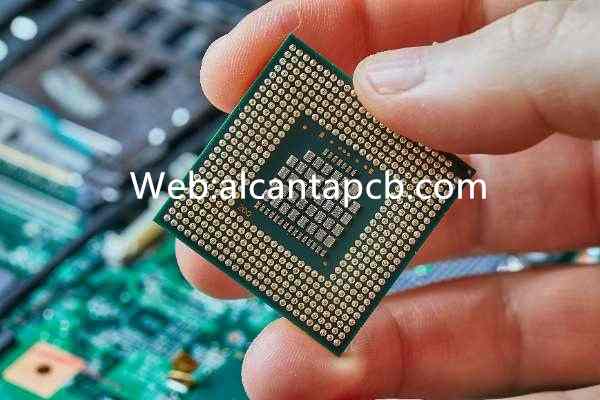
多層負荷 PCB は現代のエレクトロニクス開発の基礎です, 特に複雑な回路を必要とするシステムでは, 高い信頼性, 堅牢なパフォーマンス. これら プリント基板, 絶縁材料で分離された複数の導電性トレース層を持つ, 要求の厳しい電気負荷を処理できるように設計されています, ハイパフォーマンス コンピューティングに不可欠なものとなっています, 電気通信, および産業用途. 電子機器が進化し続ける中、, 効率的な必要性, 信頼性のある, 大容量 PCB の重要性がますます高まっています, 多層負荷 PCB テクノロジーの革新を推進.
多層負荷基板とは?
多層負荷 プリント基板 3つ以上の導電層で構成されるプリント基板です。, 通常は銅で作られています, 絶縁層によって分離されている. これらのボードは、単層または二層 PCB よりも高い電気負荷とより複雑な回路を管理するように設計されています。. 追加のレイヤーにより、より複雑なデザインが可能になります, コンポーネント密度の向上, 電気的性能の向上, 高度な電子アプリケーションに適したものにする.
多層負荷 PCB の主な利点は、コンパクトなスペース内で複雑な電気接続をサポートできることにあります。. これは、複数の層の導電経路を積み重ねることによって実現されます。, ビア(導電性材料で満たされた小さな穴)を介して相互接続されています。. 複数の層を使用すると、PCB の電気信号処理能力が向上するだけでなく、回路の全体的な完全性と信頼性も向上します。.
多層負荷基板の特徴
多層負荷 PCB は、高性能アプリケーションに適したいくつかの特徴を備えています。:
複数の層を積層できるため、より多くの回路を単一の基板に統合できます。. これは、スペースが限られているアプリケーションで特に有益です, ただし高機能が求められる.
複数のレイヤーがある場合, 設計者は特定のレイヤーをパワー専用にできる, 地面, および信号ルーティング, 電磁干渉を軽減します (EMI) 信号間のクロストーク. これにより、信号がクリーンで歪みのない状態に保たれます。, 複雑な回路でも.
多層負荷 PCB により、ボード全体へのより効率的な電力分配が可能になります. 専用の電源プレーンとグランドプレーンを使用する, PCB はより大きな電流を処理し、電力をより均一に分配できます。, ホットスポットのリスクを軽減し、安定した動作を保証します。.
複数の回路を単一の多層 PCB に結合することによって, 電子機器全体のサイズと重量を削減できます。. これはモバイルデバイスなどのアプリケーションでは特に重要です, 航空宇宙, および自動車エレクトロニクス, スペースと重量が重要な要素となる場合.
多層負荷 PCB は高い信頼性を実現するように設計されています, 追加のレイヤーにより冗長性が提供され、障害のリスクが軽減されます。. 先進的な材料と製造プロセスの使用により、厳しい環境におけるこれらのボードの耐久性とパフォーマンスがさらに向上します。.
多層負荷基板の製造プロセス
多層負荷 PCB の製造は、いくつかのステップを含む複雑なプロセスです。, それぞれがボードのパフォーマンスと信頼性を確保するために重要です:
このプロセスは、専用ソフトウェアを使用した PCB レイアウトの設計から始まります。. これには、回路の詳細な計画を作成することが含まれます。, コンポーネントの配置も含めて, トレースのルーティング, そしてレイヤーの配置. 設計ではシグナルインテグリティなどの要素を考慮する必要があります, 配電, および熱管理.
多層負荷 PCB の製造では材料の選択が重要です. 通常、導電層には高品質の銅が使用されます, 一方、絶縁層はFR4などの材料で作られています。, ポリイミド, またはその他の高性能基板. 材料はアプリケーションの特定の要件に基づいて選択する必要があります, 熱性能も含めて, 機械的強度, および電気的特性.
材料が選択されたら, 個々の層が製造される. 導電パターンは銅層にエッチングされます, そして絶縁層が適用されます. これらのレイヤーは正しい順序で積み重ねられます, ビアとスルーホールが層を適切に接続するために必要な位置合わせを行います。.
積み重ねられた層にはラミネート加工が施されます, 高圧と高温の下でそれらが一緒に押し付けられるところ. これにより、レイヤーが単一のレイヤーに結合されます。, 固体PCB. ラミネートプロセスは、剥離などの欠陥を防ぐために慎重に制御する必要があります。, 反る, または不整合.
ラミネート後, PCB に穴を開け、ビアとスルーホールを作成します。. これらの穴は導電性材料でメッキされます。, 通常は銅, 層間に必要な電気的接続を作成するため.
その後、PCB に表面仕上げ処理が施されます。, これには、はんだマスクの適用が含まれる場合があります。, シルクスクリーン印刷, HASL などの表面仕上げの蒸着 (熱風はんだレベリング), 同意する (無電解ニッケル浸漬金), または、はんだ付け性を高め、銅を酸化から保護するその他のコーティング.
最終的な PCB は厳格なテストを受け、要求仕様を満たしていることを確認します。. これには、導通をチェックするための電気テストが含まれます。, 短絡, とインピーダンス, 機械的および熱的性能を評価するための目視検査と信頼性テストだけでなく、.
多層負荷PCBのアプリケーション
多層負荷 PCB は幅広いアプリケーションで使用されます, 特に高性能の場合, 信頼性, コンパクトなサイズが求められます:
高性能コンピューティング システムにおいて, サーバーやワークステーションなど, 多層負荷 PCB は、最新のプロセッサに関連する複雑な回路と高い電気負荷を管理するために不可欠です, メモリモジュール, およびその他の重要なコンポーネント.
多層負荷 PCB は通信機器で広く使用されています, ベースステーションを含む, ルーター, とスイッチ. これらの PCB は、最新の通信ネットワークに必要な高速データ伝送と複雑な信号処理をサポートします。.
自動車エレクトロニクス分野, 多層負荷 PCB は先進運転支援システムで使用されています (ADAS), エンジンコントロールユニット (ECU), およびインフォテイメント システム. これらの PCB は、過酷な自動車環境での動作に必要な信頼性と性能を提供します。, 高温の場所, 振動, 電気ノイズがよく発生します.
多層負荷 PCB は産業用制御システムで使用されます, 自動化に必要な複雑な回路を管理する場所, ロボット工学, およびプロセス制御. これらの PCB は、産業環境の厳しい条件に耐えられるよう、信頼性と耐久性がなければなりません。.
多層負荷 PCB の利点
多層負荷 PCB には、要求の厳しい電子アプリケーションに適したいくつかの重要な利点があります。:
複数の回路を単一の基板に統合できるため、電子デバイス全体のサイズと重量が削減されます。, よりコンパクトでポータブルになります.
多層負荷 PCB により電気的性能が向上, シグナルインテグリティの向上を含む, 配電, および熱管理. そのため、信頼性と効率が重要な高性能アプリケーションに最適です。.
多層負荷 PCB は高い信頼性を実現するように設計されています, 追加のレイヤーにより冗長性が提供され、障害のリスクが軽減されます。. これにより長期稼働が保証され、メンテナンスコストが削減されます。.
複数の層を使用することで、PCB 設計の柔軟性が向上します。, より複雑な回路とシールドなどの追加機能の統合が可能になります。, 接地, そして配電.
よくある質問
多層負荷 PCB を使用する主な利点は何ですか?
多層負荷 PCB により回路密度が向上, 信号の整合性が向上しました, 強化された電力配分, 小型化と軽量化, そしてより高い信頼性, 高性能アプリケーションに最適です.
多層負荷PCBが一般的に使用されている業界は何ですか?
多層負荷 PCB は、ハイパフォーマンス コンピューティングなどの業界で一般的に使用されています。, 電気通信, 自動車エレクトロニクス, および産業制御システム, 複雑な回路と高い電気負荷を管理する場所.
多層負荷 PCB はどのように製造されるのか?
製造プロセスにはデザインとレイアウトが含まれます, 材料の選択, レイヤースタッキング, ラミネート加工, 穴あけとメッキ, 表面仕上げ, パフォーマンスと信頼性を確保するための厳格なテスト.
多層負荷 PCB においてシグナルインテグリティが重要な理由?
多層負荷 PCB では、電気信号がクリーンで歪みのない状態を維持できるようにするために、信号の完全性が非常に重要です。, 電磁干渉と信号間のクロストークのリスクを軽減します。.