株式会社")
多層負荷試験 PCB メーカー。多層負荷試験 PCB メーカーは、さまざまな電気負荷を処理およびテストするように設計された高性能プリント基板の製造を専門としています。. これらのメーカーは、ストレス下で電子デバイスの信頼性と耐久性を確保するために不可欠な多層 PCB を製造しています。. 高度な設計と負荷テストの精度により、実際の動作条件の正確なシミュレーションが可能になります。, PCB の性能と寿命についての貴重な洞察を提供します。. このテストは、電気通信などの重要な分野のアプリケーションにとって非常に重要です。, 航空宇宙, 自動車産業.
多層負荷試験 PCB は、さまざまな負荷条件下で電子コンポーネントおよびシステムの性能を評価および検証するように設計された特殊なプリント基板です。. これら プリント基板 複雑な電子デバイスの開発および製造プロセスに不可欠です, すべてのコンポーネントがストレス下でも確実に動作することを保証する. 複数層の回路と相互接続を処理できるため、これらの PCB は高度なテスト シナリオに対応できます。, 電気通信などの産業に欠かせないものとなっています, 航空宇宙, およびコンシューマーエレクトロニクス.
多層負荷試験PCBとは何ですか?
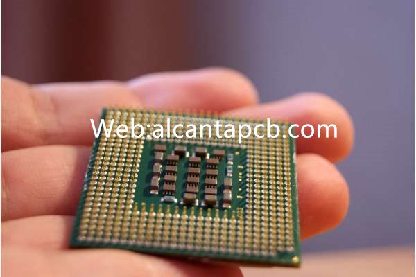
多層負荷テスト プリント基板 複数の層の導電経路と絶縁材料を備えたプリント回路基板です。, 電子コンポーネントおよびシステムの耐荷重能力をテストするために特別に設計されています. 単層または二層 PCB とは異なります, 多層 PCB は 3 つ以上の層で構成されます, 各層には独自の回路と接続のセットが含まれています. これらの層を積層し、絶縁材で接着します。, 複雑な試験手順に対応できるコンパクトで複雑な構造を形成.
多層負荷テスト PCB の主な機能は、実際の動作条件をシミュレートし、さまざまな負荷の下で電子コンポーネントがどのように動作するかを評価することです。, 電流などの, 電圧, 熱応力と. これらの条件を再現すると、, エンジニアは潜在的な弱点を特定できる, コンポーネントのパフォーマンスを最適化する, 最終製品がすべての信頼性と安全性基準を満たしていることを確認します。.
多層負荷試験用PCBの特徴
多層負荷試験 PCB は、厳密な試験用途に適したいくつかの重要な特性を備えています。:
これらの PCB の複数の層により、高密度の接続と回路が可能になります。, 多数のコンポーネントと相互接続を伴う複雑なテストシナリオを可能にする. この高密度は、最新の電子デバイスをテストするために非常に重要です, 多くの場合、コンパクトなスペースに多数のコンポーネントが統合されています。.
多層負荷試験 PCB は、高周波試験条件下でも信号の完全性を維持するように設計されています。. レイヤー内でのグランドプレーンと電源プレーンの慎重な配置により、ノイズが最小限に抑えられます。, クロストーク, と信号損失, 正確で信頼性の高いテスト結果を保証する.
負荷テストでは効果的な熱管理が不可欠です, コンポーネントはストレス下でかなりの熱を発生する可能性があるため、. これらの PCB はサーマルビアを使用して設計されています, ヒートシンク, 熱を効率的に放散するためのその他の熱管理機能, テスト中のコンポーネントへの損傷を防止します.
多層負荷試験 PCB は、試験手順に伴う機械的ストレスに耐えるように構築されています, コンポーネントの繰り返しの挿入と取り外しなど, 振動, 温度サイクルと. これらの PCB の堅牢な構造により、テストプロセス全体にわたって構造的完全性が維持されます。.
これらの PCB は、特定のテスト要件を満たすようにカスタマイズできます。, レイヤー数も含めて, 材料の種類, そして回路のレイアウト. この柔軟性により、エンジニアは各テスト シナリオの固有の要求に合わせた PCB を設計できます。, 大電流試験が含まれるかどうか, RF信号評価, または熱応力解析.
多層負荷試験用基板の製造工程
多層負荷試験 PCB の製造には、正確で複雑ないくつかの手順が含まれます:
このプロセスは、専用の CAD ソフトウェアを使用した PCB の設計とレイアウトから始まります。. エンジニアは、テスト手順に必要な回路と相互接続の概要を示す詳細な回路図を作成します。. 設計ではシグナルインテグリティなどの要素を考慮する必要があります, 熱管理, 機械的安定性.
特定のテスト要件に基づいて高品質の材料が選択されます. 一般的な材料には、一般用途向けの FR4 が含まれます, 高周波試験用PTFE, 熱伝導率を高めるための金属コア. 材料の選択は、負荷テスト中の PCB のパフォーマンスと信頼性に影響します。.
PCB 層は特定の順序で積み重ねられます, 各導電層の間に絶縁材料が配置されている. スタックアップ設計は、望ましい電気的性能を達成するために重要です, インピーダンスなどの要素に影響を与えるため, シグナルインテグリティ, および熱管理.
積み重ねられた層は高圧および高温下で積層されます。, 強固で凝集性のある PCB 構造の作成. ラミネートプロセスにより、層が確実に接着されます。, 試験中の層間剥離や反りを防止.
PCB に穴を開けてビアを作成します, 異なる層を電気的に接続します. これらのビアは導電性材料でメッキされます。, 銅などの, 層間の信頼性の高い電気接続を確保するため.
回路パターンは化学プロセスを使用して銅層にエッチングされます。. このステップでは、テスト中に信号と電力を伝導するために使用される電気経路を定義します。.
PCBは保護コーティングで仕上げられています, はんだマスクなど, そして表面仕上げ, エニグなど (無電解ニッケル浸漬金), 銅回路を酸化から保護し、はんだ付け性を向上させます。.
ついに, PCB は必要なコンポーネントで組み立てられ、すべての性能仕様を満たしていることを確認するために厳格なテストを受けます。. これには電気試験が含まれる場合があります, 熱試験, PCB が意図した負荷条件に耐えられることを検証するための機械的テスト.
多層負荷試験 PCB のアプリケーション
多層負荷試験 PCB は、電子部品の性能と信頼性が重要となるさまざまなアプリケーションで使用されます。:
電気通信業界では, これらの PCB は、アンプなどのコンポーネントの耐荷重能力をテストするために使用されます。, フィルター, およびトランシーバー. 高周波信号を処理し、信号の完全性を維持する能力は、信頼性の高い通信を確保するために重要です。.
航空宇宙および防衛用途では、多くの場合、コンポーネントが極端な条件下で動作する必要があります。, 高温を含む, 振動, そして放射線. 多層負荷試験 PCB は、これらの条件をシミュレートし、アビオニクスの性能を検証するために使用されます。, レーダーシステム, およびその他の重要な電子機器.
自動車エレクトロニクス分野, これらの PCB は、エンジン コントロール ユニットなどのコンポーネントの耐久性と信頼性をテストするために使用されます。, センサー, およびインフォテイメント システム. 熱サイクルに耐える能力, 機械的ストレス, 電気負荷は自動車システムの安全性とパフォーマンスを確保するために不可欠です.
多層負荷試験 PCB は家庭用電化製品の開発にも使用されています, スマートフォンなどの, 錠剤, およびウェアラブル. これらのデバイスは多くの場合、コンパクトなフォームファクターに多数のコンポーネントを統合しています。, さまざまな負荷条件下でのパフォーマンスを検証することが不可欠です.
多層負荷試験 PCB の利点
多層負荷試験 PCB には、厳格な試験用途に理想的な選択肢となるいくつかの利点があります。:
回路と相互接続の複数の層により、包括的なテストシナリオが可能になります, エンジニアがさまざまな負荷条件下で複雑な電子システムのパフォーマンスを評価できるようにします.
これらの PCB の慎重な設計とレイアウトにより、高周波テスト条件下でも信号の完全性が維持されることが保証されます。, 正確で信頼性の高いテストデータが得られます.
これらの PCB の高度な熱管理機能は、負荷テスト中の過熱の防止に役立ちます, PCB とコンポーネントの両方を熱損傷から保護します。.
PCB 設計と材料をカスタマイズできるため、エンジニアは特定のテスト ニーズに合わせたソリューションを作成できます。, PCB がすべての性能と信頼性の要件を満たしていることを確認する.
よくある質問
多層負荷テスト PCB の主な目的は何ですか?
多層負荷テスト PCB の主な目的は、さまざまな負荷条件下で電子コンポーネントおよびシステムのパフォーマンスを評価および検証することです。, 現実世界の運用シナリオに耐えられることを保証する.
多層負荷テスト PCB はテスト中に信号の整合性をどのように維持するのか?
信号の完全性は、慎重な設計とレイアウトによって維持されます。, グランドプレーンと電源プレーンの戦略的な配置を含む, 騒音を最小限に抑えるために先進的な材料と製造技術を使用しています。, クロストーク, と信号損失.
多層負荷試験 PCB から最も恩恵を受けるのはどの業界ですか?
電気通信などの産業, 航空宇宙, 防衛, 自動車エレクトロニクス, これらの PCB から最も恩恵を受けるのは家庭用電化製品です。, 製品の信頼性と性能を保証するために厳格なテストが必要なため.
多層負荷テスト PCB を特定のアプリケーション向けにカスタマイズできますか?
はい, これらの PCB は、特定のテスト要件を満たすように高度にカスタマイズできます, レイヤー数も含めて, 材料の種類, 回路レイアウト, および熱管理機能, エンジニアがテストのニーズに合わせてカスタマイズされたソリューションを設計できるようにする.