株式会社")
パッケージテスト基板メーカー.A パッケージ テスト回路基板メーカーは、半導体パッケージのテストに合わせた高品質の回路基板の設計と製造を専門としています。. これらのボードは、さまざまなパッケージング技術の包括的な電気評価と熱評価を促進することにより、最適なパフォーマンスと信頼性を保証します. 精密エンジニアリングと高度な製造プロセスを備えています, これらの回路基板は、複数の業界にわたる半導体デバイスの機能と耐久性を検証する上で重要な役割を果たします。.
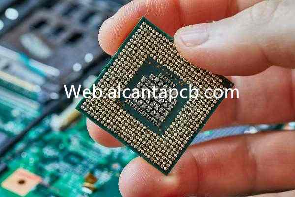
パッケージテスト回路基板は、集積回路の性能と信頼性をテストおよび検証するために半導体業界で使用される重要なツールです (IC) パッケージ. これらの特殊なボードは、さまざまな IC パッケージに対応できるように設計されています。, ボールグリッドアレイを含む (BGA), クワッドフラットパッケージ (MF), およびチップスケールパッケージ (CSP). パッケージテスト回路基板の主な機能は、IC を実装し、さまざまな電気的検査を受けることができるプラットフォームを提供することです。, 熱, 最終製品に組み込まれる前の機械的テスト. これにより、完全に機能し信頼性の高い IC のみが製造プロセスに進むことが保証されます。, これにより、エンドユーザー アプリケーションの障害のリスクが軽減されます。.
パッケージテスト基板とは?
パッケージテスト回路基板は、特別に設計されたプリント回路基板です。 (プリント基板) 現実的な動作条件下で IC パッケージをテストするために使用されます. これらのボードは、IC が最終的に機能する環境を再現するように設計されています。, メーカーが電気的性能を評価できるようにする, シグナルインテグリティ, およびパッケージの熱管理. 基板レイアウトには通常、自動テスト装置と接続できるテスト ソケットまたはその他の形式のコネクタが含まれています。 (食べた). このセットアップにより、複数の IC の迅速なテストが可能になります。, 各パッケージのパフォーマンスに関する貴重なデータを提供します.
これらのボードは、半導体製造における品質保証プロセスに不可欠です。. はんだ接合の完全性の低下などの問題を特定するのに役立ちます。, 熱応力の問題, および電気的性能の異常, 梱包プロセス中に発生する可能性があります. こういった問題を早期に発見することで、, パッケージテスト回路基板は、最終製品の信頼性と寿命を確保する上で重要な役割を果たします。.
材料と設計の考慮事項
パッケージテスト回路基板の材料と設計は、その性能にとって非常に重要です。. これらのボードは通常、高品質 FR4 材料、または Rogers や Taconic ラミネートなどのその他の先進的な基板を使用して構築されます。, 優れた電気的および熱的特性を提供します. 材料の選択は、テストされる IC パッケージの特定の要件によって決まります。, 動作頻度も含めて, 消費電力, および機械的ストレス耐性.
素材選びに加えて, パッケージテスト回路基板の設計では、次の要素を考慮する必要があります。:
PCB 上の配線レイアウトは、信号損失と干渉を最小限に抑えるために細心の注意を払って設計する必要があります。. 高周波IC, 特に, テスト中に信号の完全性を維持するには、制御されたインピーダンス配線と適切な接地が必要です.
効果的な熱管理が重要です, 特に動作中にかなりの熱を発生する IC の場合. PCB にはサーマルビアが含まれる場合があります, ヒートシンク, 熱を放散し、テスト中の IC への熱損傷を防ぐその他のメカニズム.
ボードは、テスト中の IC パッケージの繰り返しの挿入と取り外しに耐えられるように機械的に堅牢である必要があります。. これには基板の厚さを慎重に考慮する必要があります, コネクタ部分の補強, ソルダーマスクの耐久性.
パッケージテスト回路基板は多くの場合、多用途に使えるように設計されています, さまざまなICパッケージのタイプとサイズに対応. この柔軟性はモジュール式テストソケットによって実現されます。, 調整可能な取り付け機構, 適応可能な PCB レイアウト.
パッケージテスト基板の製造工程
パッケージテスト回路基板の製造プロセスは標準的な PCB の製造プロセスと似ていますが、半導体テストの厳しい要件を満たすために追加の精度と品質管理ステップが追加されています。:
プロセスは設計段階から始まります, 特定の IC パッケージとテスト要件に一致するようにボード レイアウトが作成される場所. プロトタイピングには、初期テストと検証用の少数の基板の作成が含まれます。.
設計に基づいて, 適切な材料が選択されています, そして基板が準備されます. これには、選択した材料を銅層でラミネートし、必要なコーティングを適用することが含まれます。.
フォトリソグラフィー技術を用いて回路パターンを基板上に転写します。, 続いてエッチングを行って余分な銅を除去し、目的のトレース パターンを作成します。.
ビアを作成するために穴が開けられます, その後、PCB の異なる層間に電気接続を確立するためにメッキされます。.
表面仕上げ, エニグなど (無電解ニッケル浸漬金), 露出した銅を保護し、はんだ付け性を向上させるために適用されます。.
テストソケット, コネクタ, およびその他のコンポーネントが基板に実装されている. 組み立てプロセスは正確に実行され、すべてのコンポーネントがしっかりと取り付けられ、適切に位置合わせされていることを確認します。.
完成したボードは厳格なテストを受け、すべての仕様を満たしていることを確認します。. これには、トレースの導通性とインピーダンスを検証するための電気テストが含まれます。, 耐久性を評価するための機械的試験だけでなく.
パッケージテスト基板の用途
パッケージテスト回路基板は、半導体業界でさまざまなテスト目的で広く使用されています。:
これらのボードを使用すると、メーカーは IC の電気的性能をテストできます。, 電圧などのパラメータを含む, 現在, シグナルインテグリティ. これにより、IC が大規模なシステムに統合される前に、必要な仕様を確実に満たすことができます。.
パッケージテスト回路基板は、ICパッケージの熱性能を評価するために使用されます。. これには、動作条件下でのパッケージの熱放散能力のテストが含まれます。, これは熱関連の故障を防ぐために重要です.
ICパッケージの機械的堅牢性は、ストレステストを受けることによってテストされます。, 振動も含めて, ショック, 挿入/取り外しサイクルの繰り返し. これは、パッケージ設計または製造プロセスにおける潜在的な弱点を特定するのに役立ちます。.
長期信頼性テストは、パッケージテスト回路基板を使用して実施され、IC がその寿命にわたって経験する動作条件をシミュレートします。. これには熱サイクルのテストが含まれます, 耐湿性, および電気的耐久性.
パッケージテスト基板を使用する利点
パッケージテスト回路基板を使用すると、半導体製造においていくつかの利点が得られます:
パッケージレベルでICをテストすることにより, メーカーは、IC が最終製品に組み込まれる前に問題を特定して対処できます。. これにより、費用のかかるリコールや現場での製品故障のリスクが軽減されます。.
パッケージテスト回路基板により、IC の性能を詳細に分析できるため、包括的な品質管理が可能になります, 熱挙動, 機械的完全性.
これらのボードは、大量の IC をテストするためのコスト効率の高いソリューションを提供します。, 複数回再利用でき、さまざまな種類のパッケージのテストに適応できるため.
厳格なテストを経て, パッケージテスト回路基板は、最も信頼性の高い IC のみが最終製品に採用されることを保証します。, 電子システム全体の信頼性とパフォーマンスを向上させる.
よくある質問
パッケージテスト回路基板に通常使用される材料は何ですか?
FR4などの材質, ロジャース, Taconic ラミネートは、優れた電気的および熱的特性により一般的に使用されます。.
パッケージテスト回路基板で熱管理が重要な理由?
効果的な熱管理により、テスト中の過熱を防止します。, これは、IC パッケージの完全性を維持し、正確なテスト結果を保証するために重要です。.
1 つのパッケージ テスト回路基板でさまざまな種類の IC パッケージをテストできますか?
はい, 多くのパッケージテスト回路基板は多用途に使えるように設計されています, モジュール式テストソケットと適応性のあるレイアウトにより、さまざまな IC パッケージのタイプとサイズに対応できるようになります。.
パッケージテスト回路基板は製品の信頼性にどのように貢献しますか?
問題の早期発見と包括的なテストを可能にすることにより、, これらのボードは、完全に機能し信頼性の高い IC のみが最終製品に使用されるようにするのに役立ちます。, 現場での失敗の可能性を減らす.