株式会社")
ミリ波アンテナPCBメーカー。主要なワイヤボンディングIC基板メーカーとして, 信頼できる接続と最適な電気性能を確保する高性能基板の生産を専門としています. 当社の高度な製造プロセスと厳しい品質管理基準は、最高の業界要件を満たす基質を保証します, エレクトロニクス分野の幅広いアプリケーションをサポート.
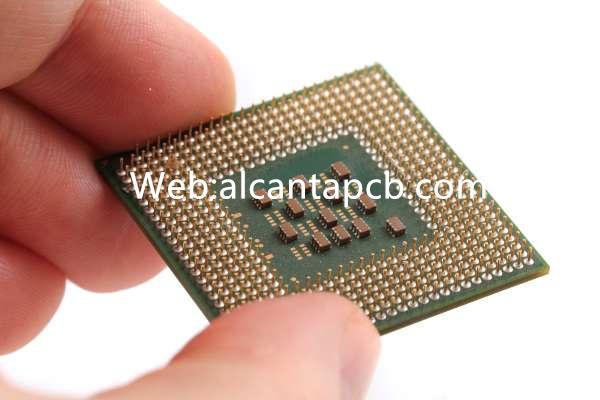
ミリ波アンテナ プリント基板 (プリント基板) 高周波通信システムの設計と展開における重要なコンポーネントです, 特にミリ波スペクトルでは, からの範囲 30 GHzから 300 GHz. これらの PCB は、ミリ波信号の送受信をサポートするように設計されています。, 5G ネットワークなどのアプリケーションに不可欠なものとなっています, レーダーシステム, 衛星通信, 高度な画像技術と. ミリ波アンテナ PCB の設計と材料の選択は、信号の整合性を維持するために重要です。, 損失を最小限に抑える, 高周波環境でも信頼性の高いパフォーマンスを保証します.
ミリ波アンテナ基板とは?
ミリ波アンテナ プリント基板 ミリ波周波数で動作するように設計された特殊なタイプのプリント基板です。. これらの周波数, 従来の RF およびマイクロ波アプリケーションで通常使用されるものよりも高い, 関連する課題に対処するには、細心の注意を払った設計と製造技術が必要です, 信号の減衰など, インピーダンスマッチング, および熱管理.
PCB は、アンテナおよびその他の高周波コンポーネントのプラットフォームとして機能します。, 必要な電気的相互接続と機械的サポートを提供する. アンテナの設計, パッチアンテナを含めることができます, マイクロストリップアンテナ, または他のタイプのミリ波アンテナ, 望ましい放射パターンと信号性能を達成するために PCB に統合されています.
ミリ波アンテナの基板に使用される材料
高周波数での最適な性能を確保するには、ミリ波アンテナ PCB の材料の選択が重要です。. 誘電率などの主要な材料特性, 損失正接, 熱安定性を慎重に考慮する必要があります. 一般的な資料には含まれます:
PTFEベースのラミネート, ロジャースRT/デュロイドなど 5880, 誘電率が低く、損失正接が非常に低いため、ミリ波アプリケーションで広く使用されています。. これらの特性は、信号損失を最小限に抑え、高い信号整合性を維持するのに役立ちます。, PTFE が高周波 PCB 設計に好ましい選択肢となる.
強化された機械的安定性と熱的性能を必要とする用途向け, セラミック入りPTFEラミネートを使用. これらの材料は、純粋な PTFE の低損失特性を維持しながら、寸法安定性と熱伝導率を向上させます。.
LCP は、優れた高周波性能によりミリ波 PCB で使用されるもう 1 つの材料です。, 吸湿性が低い, 優れた熱安定性. LCP はミリ波アプリケーションのフレキシブルおよびリジッドフレックス設計に特に適しています.
LTCC基板は、高精度と信頼性が要求される高周波アプリケーションで使用されます。. LTCC 材料は優れた熱伝導率を提供し、埋め込まれた受動部品と同時焼成できます。, コンパクトに最適です, 高密度設計.
ミリ波アンテナ PCB の設計上の考慮事項
ミリ波アンテナ PCB の設計には、いくつかの重要な要素に細心の注意を払う必要があります:
アンテナは PCB の重要なコンポーネントです, そしてその設計は特定の周波数範囲と用途に合わせて最適化する必要があります. アンテナの種類の選択 (例えば。, パッチ, マイクロストリップ) 望ましい放射パターンを実現し、信号損失を最小限に抑えるには、PCB 上の配置とその配置が重要です。.
アンテナと伝送線路間の効率的な電力伝送を確保するには、インピーダンス整合が不可欠です。, 信号反射を最小限に抑え、信号強度を最大化します。. これにはトレースの寸法を正確に制御する必要があります, 間隔, 適切なインピーダンス整合技術の使用.
ミリ波周波数では, 信号減衰の増加と潜在的な干渉により、信号の完全性を維持するのは困難です. PCB レイアウトは寄生効果を最小限に抑える必要があります, クロストーク, そして放射線損失. 適切な接地, シールド, 信号の完全性を維持するには高品質の素材の使用が不可欠です.
高周波信号はかなりの熱を発生する可能性があります, 特に電力を大量に消費するアプリケーションでは. 効果的な熱管理戦略, 熱伝導率の高い素材を使用するなど, ヒートシンクの追加, またはサーマルビアを組み込む, 過熱を防止し、長期的な信頼性を確保するために必要です.
多層ミリ波 PCB の層の積層は、伝送線路のインピーダンスを制御し、信号損失を最小限に抑えるために慎重に設計する必要があります。. 信号の整合性を維持するには、専用のグランド プレーンの使用と層間の制御された誘電体間隔が重要です。.
ミリ波アンテナ基板の製造工程
ミリ波アンテナ PCB の製造には、基板が高周波動作の厳しい要件を確実に満たすようにするための特殊なプロセスが含まれます。:
このプロセスは、適切な基板材料を選択して準備することから始まります。, 高周波性能に影響を与える可能性のある欠陥がないことを確認する.
アンテナと回路パターンは高度なフォトリソグラフィーとエッチング技術を使用して作成されます。. このステップの精度は非常に重要です, あらゆる変動がアンテナのパフォーマンスと全体的な信号の完全性に影響を与える可能性があるため、.
マイクロビアは、層間接続を作成するためにミリ波 PCB でよく使用されます。. これらのビアは高精度で穴あけされ、信頼性の高い電気接続を確保するためにメッキされています。.
多層設計の場合, 層は高圧および高温下で積層されます。. このステップでは、望ましい電気的および機械的特性を維持するために慎重な制御が必要です。.
PCB 上の露出した銅は表面仕上げでコーティングされています, エニグなど (無電解ニッケル浸漬金) またはイマージョンシルバー, トレースを保護し、良好なはんだ付け性を確保するため.
完成した PCB は厳格なテストを受けます, インピーダンス測定を含む, シグナルインテグリティ解析, および熱サイクル試験, ミリ波アプリケーションに必要な仕様を満たしていることを確認するため.
ミリ波アンテナ基板の応用例
ミリ波アンテナ PCB はさまざまな高度なアプリケーションで使用されています, 含む:
これらの PCB は 5G インフラストラクチャにおいて重要です, 超高速データ伝送と低遅延接続に必要な高周波通信を可能にします。.
ミリ波PCBは衝突回避用の自動車レーダーシステムに使用されています, アダプティブクルーズコントロール, およびその他の先進運転支援システム (ADAS).
衛星システム内, ミリ波 PCB は高周波通信リンクを促進します, 信頼性の高い高速データ伝送を提供します.
ミリ波PCBは高度な画像技術で使用されています, セキュリティスキャナーや医療用画像装置など, 高解像度および高周波信号が必要な場合.
ミリ波アンテナ基板のメリット
ミリ波アンテナ PCB にはいくつかの利点があります, 高周波アプリケーションに不可欠なものとなっています:
これらの PCB は、次の周波数まで処理できるように設計されています。 300 GHz, 最小限の信号損失と高い信号の完全性を確保します.
これらの PCB に使用される材料と製造プロセスは、高い精度と信頼性を実現します。, これは、厳しい条件下で一貫したパフォーマンスを必要とするアプリケーションにとって重要です。.
効果的な熱管理戦略が設計と材料に組み込まれています, PCB が過熱することなく高電力レベルを処理できるようにする.
アンテナを PCB に直接統合できるため、よりコンパクトで効率的な設計が可能になります。, これは現代の通信デバイスやシステムにおいて特に重要です.
よくある質問
ミリ波アンテナの PCB に一般的に使用される材料は何ですか?
一般的な材質には PTFE が含まれます, セラミック充填PTFE, 液晶ポリマー (LCP), および低温同時焼成セラミックス (LTCC), 低い誘電損失と高い熱安定性のために選ばれました.
ミリ波アンテナ PCB でインピーダンス整合が重要な理由?
インピーダンスマッチングにより効率的な電力伝送が保証され、信号反射が最小限に抑えられます。, これは高周波での信号強度と完全性を維持するために重要です.
ミリ波アンテナ PCB を使用するアプリケーション?
これらの PCB は 5G ネットワークで使用されます, レーダーシステム, 衛星通信, および高度な画像システム.
ミリ波アンテナ PCB で信号の完全性はどのように維持されるか?
慎重な PCB レイアウトにより信号の整合性が維持されます, 高品質の素材の使用, 適切な接地, およびインピーダンス制御, これらすべてが信号損失と干渉を最小限に抑えるのに役立ちます.