CO.,LTD")
Produttore di PCB a radiofrequenza. Come radio leader Frequenza Produttore di PCB, siamo specializzati nella produzione di PCB RF di alta qualità su misura per soddisfare i requisiti esigenti dei moderni sistemi di comunicazione. I nostri processi di produzione avanzati garantiscono un'eccellente integrità del segnale, bassa perdita, e alta affidabilità. Sia per le reti 5G, comunicazioni satellitari, o applicazioni militari, i nostri PCB RF offrono prestazioni e durata superiori, rendendoci la scelta preferita per soluzioni tecnologiche all’avanguardia.
Radiofrequenza (RF) I PCB sono circuiti stampati specializzati progettati per funzionare ad alte frequenze. Queste schede sono fondamentali nelle applicazioni in cui è richiesta una gestione precisa ed efficiente dei segnali in radiofrequenza, come nel caso delle telecomunicazioni, reti senza fili, sistemi radar, e altre applicazioni ad alta frequenza. I PCB RF sono costruiti con materiali e design unici per garantire una perdita minima di segnale, elevata integrità del segnale, e prestazioni affidabili in ambienti esigenti.
Cos'è un PCB a radiofrequenza?
Una RF PCB è un tipo di circuito stampato appositamente progettato per gestire segnali ad alta frequenza, tipicamente nell'ordine dei megahertz (MHz) a gigahertz (GHz). Questi PCB vengono utilizzati in dispositivi e sistemi in cui la trasmissione e la ricezione delle onde radio sono essenziali. La progettazione e la costruzione dei PCB RF richiedono un'attenzione meticolosa ai materiali, disposizione, e processi di produzione per ottenere le prestazioni elettriche e l'affidabilità desiderate.
La progettazione di un PCB RF implica diverse considerazioni critiche per garantire prestazioni ottimali alle alte frequenze. Le sezioni seguenti descrivono gli aspetti chiave della progettazione PCB RF.
I materiali utilizzati nei PCB RF svolgono un ruolo significativo nelle loro prestazioni. I materiali primari includono:
Materiali del substrato: Substrati ad alta frequenza come Rogers, PTFE (Teflon), e i materiali riempiti di ceramica sono comunemente usati a causa della loro bassa costante dielettrica (Non so) e basso fattore di dissipazione (Df). Questi materiali aiutano a mantenere l'integrità del segnale alle alte frequenze.
Lamina di rame: Per le tracce e i piani conduttivi viene utilizzato rame di elevata purezza, fornendo eccellente conduttività elettrica e affidabilità.
Preimpregnato e laminato: Per unire insieme gli strati vengono utilizzati materiali preimpregnati e laminati ad alte prestazioni, offrendo bassa perdita dielettrica ed elevata stabilità termica.
L'impilamento dei livelli è un aspetto cruciale della progettazione PCB RF:
Strati di segnale: Per instradare i segnali ad alta frequenza vengono utilizzati più livelli di segnale. Questi strati sono progettati con impedenza controllata per garantire una perdita minima di segnale e un'elevata integrità del segnale.
Aerei di potenza e di terra: I piani di alimentazione e di terra dedicati forniscono riferimenti di tensione stabili e riducono il rumore, che è fondamentale per mantenere l'integrità del segnale nelle applicazioni RF.
Strati di gestione termica: Sono incorporati canali termici e diffusori di calore per dissipare il calore generato dai componenti ad alta frequenza, garantendo prestazioni affidabili.
Durante la fase di progettazione è necessario affrontare diverse considerazioni chiave:Integrità del segnale: L'elevata integrità del segnale viene mantenuta attraverso l'impedenza controllata, instradamento di coppie differenziali, e minimizzando gli effetti parassiti. La progettazione deve garantire che i percorsi del segnale siano quanto più brevi e diretti possibile.
Distribuzione dell'energia: L'efficiente distribuzione della potenza è assicurata attraverso piani di potenza dedicati, riducendo al minimo le cadute di tensione e garantendo un'erogazione di potenza stabile ai componenti RF.
Gestione termica: Tecniche efficaci di gestione termica, quali vie termiche e diffusori di calore, prevenire il surriscaldamento e garantire prestazioni costanti.
Stabilità meccanica: La scheda deve fornire un supporto meccanico robusto per resistere alle sollecitazioni derivanti dalla movimentazione e dal funzionamento in ambienti ad alta frequenza.
Affidabilità: L'affidabilità a lungo termine è garantita dall'uso di materiali di alta qualità e processi di produzione precisi, prevenendo problemi come la delaminazione e la deformazione.
Quali materiali vengono utilizzati nei PCB RF?
I materiali utilizzati nei PCB RF sono selezionati per le loro caratteristiche elettriche, termico, e proprietà meccaniche:
Substrato di Rogers: I materiali Rogers sono ampiamente utilizzati nelle applicazioni RF grazie alla loro bassa costante dielettrica e alle basse perdite, che sono essenziali per le prestazioni ad alta frequenza.
PTFE (Teflon): Il PTFE è un'altra scelta popolare per i substrati RF, offrendo eccellenti proprietà elettriche e bassa perdita dielettrica.
Materiali riempiti con ceramica: Questi materiali forniscono un'elevata stabilità termica e una bassa perdita dielettrica, rendendoli adatti per applicazioni RF ad alta potenza.
Lamina di rame: Per le tracce e i piani conduttivi viene utilizzato rame di elevata purezza, fornendo eccellente conduttività elettrica e affidabilità.
Preimpregnato e laminato: Per unire insieme gli strati vengono utilizzati materiali preimpregnati e laminati ad alte prestazioni, offrendo bassa perdita dielettrica ed elevata stabilità termica.
Di che dimensioni sono i PCB RF?
La dimensione dei PCB RF varia a seconda dell'applicazione e dei requisiti di progettazione specifici:
Spessore: Lo spessore dei PCB RF può variare da 0.5 mm a diversi millimetri, a seconda del numero di strati e dei requisiti di gestione termica.
Dimensioni: La lunghezza e la larghezza dei PCB sono determinate dalla dimensione dei componenti e dal layout del sistema. Possono variare da fattori di forma ridotti per dispositivi compatti a schede di grandi dimensioni per sistemi RF complessi.
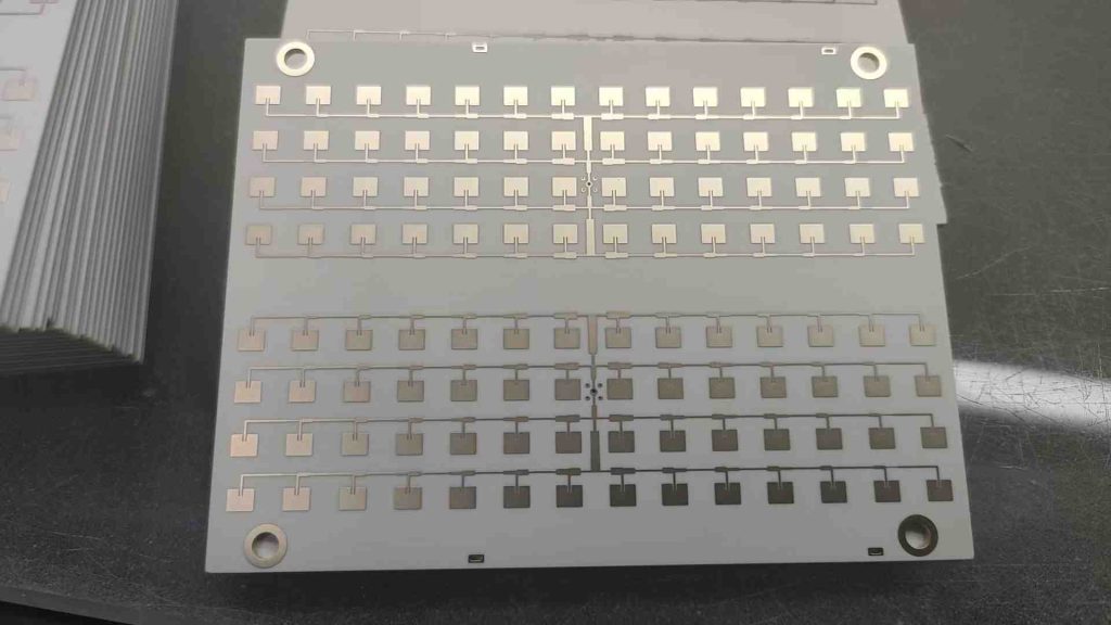
Il processo di produzione dei PCB RF
Il processo di produzione dei PCB RF prevede diverse fasi precise e controllate per garantire qualità e prestazioni elevate:
Materiali di supporto ad alte prestazioni, lamine di rame, e i materiali preimpregnati vengono preparati e tagliati in dimensioni adeguate per la lavorazione.
Gli strati vengono fabbricati laminando materiali conduttivi e isolanti in una pila. Ogni strato è modellato utilizzando la fotolitografia per definire i circuiti.
Microvie e fori passanti vengono realizzati utilizzando tecniche di perforazione laser o meccanica. Questi fori vengono poi placcati con rame per creare collegamenti elettrici tra gli strati.
I singoli strati vengono laminati insieme sotto calore e pressione per formare un solido, struttura multistrato. Questo processo garantisce che tutti gli strati siano saldamente incollati e allineati.
I processi di fotolitografia e incisione vengono utilizzati per creare circuiti a passo fine su ogni strato, che richiedono alta precisione per interconnessioni accurate.
Dopo la fabbricazione, la scheda è assemblata con tutti i componenti e connettori necessari. Vengono condotti test rigorosi per garantire che la scheda soddisfi tutte le specifiche di progettazione e i requisiti prestazionali.
L'area di applicazione dei PCB RF
I PCB RF sono utilizzati in un'ampia gamma di applicazioni ad alta frequenza:
Nelle telecomunicazioni, I PCB RF vengono utilizzati nelle stazioni base, antenne, e altre apparecchiature di comunicazione ad alta frequenza per garantire una trasmissione e una ricezione affidabili del segnale.
Nelle applicazioni aerospaziali e della difesa, I PCB RF sono utilizzati nei sistemi radar, apparecchiature di comunicazione, e sistemi di guerra elettronica, dove il controllo preciso dei segnali RF è fondamentale.
Nei dispositivi medici, I PCB RF vengono utilizzati nei sistemi di imaging, apparecchiature diagnostiche, e dispositivi di comunicazione wireless, dove le prestazioni ad alta frequenza sono essenziali.
Nelle apparecchiature di prova e misurazione, I PCB RF vengono utilizzati per supportare il test e l'analisi dei segnali ad alta frequenza, garantendo risultati accurati e affidabili.
Quali sono i vantaggi dei PCB RF?
I PCB RF offrono numerosi vantaggi che li rendono indispensabili nelle applicazioni ad alta frequenza:
Alte prestazioni: Forniscono eccellenti proprietà elettriche, consentendo una trasmissione affidabile del segnale ad alta frequenza con una perdita minima.
Integrità del segnale: L'elevata integrità del segnale viene mantenuta attraverso l'impedenza controllata e i materiali a bassa perdita, garantendo una trasmissione accurata del segnale.
Gestione termica: Efficaci tecniche di gestione termica prevengono il surriscaldamento e garantiscono prestazioni costanti alle alte frequenze.
Stabilità meccanica: Le robuste proprietà meccaniche garantiscono che la scheda possa resistere alle sollecitazioni derivanti dalla manipolazione e dal funzionamento in ambienti ad alta frequenza.
Affidabilità: Materiali di alta qualità e processi di produzione precisi garantiscono affidabilità e prestazioni a lungo termine.
Domande frequenti
Quali sono le considerazioni chiave nella progettazione di un PCB RF?
Le considerazioni chiave includono la selezione dei materiali per le prestazioni elettriche e termiche, impilamento dei livelli per routing complessi, e garantire l'integrità del segnale, distribuzione del potere, gestione termica, stabilità meccanica, e affidabilità.
In che modo i PCB RF differiscono dai PCB standard?
I PCB RF sono progettati specificamente per applicazioni ad alta frequenza, caratterizzato da materiali e design avanzati per una perdita di segnale minima, mentre i PCB standard vengono utilizzati per applicazioni elettroniche generali con requisiti prestazionali meno impegnativi.
Qual è il tipico processo di produzione dei PCB RF?
Il processo prevede la preparazione del materiale, fabbricazione dello strato, foratura e placcatura, laminazione, schema circuitale, assemblaggio, e test rigorosi per garantire qualità e prestazioni elevate.
Quali sono le principali applicazioni dei PCB RF?
Questi PCB sono utilizzati nelle telecomunicazioni, aerospaziale e della difesa, dispositivi medici, e apparecchiature di prova e misurazione, fornendo funzionalità avanzate e affidabilità nelle applicazioni ad alta frequenza.