CO.,LTD")
Produttore RF PCB. AN RF Produttore PCB è specializzato nella progettazione e produzione di circuiti stampati per applicazioni a radiofrequenza. Questi PCB sono essenziali per la trasmissione del segnale ad alta frequenza nei dispositivi di comunicazione wireless, sistemi radar, e tecnologia satellitare. Il produttore garantisce di alta qualità, Fabbricazione precisa per soddisfare i requisiti rigorosi delle prestazioni RF, inclusa l'integrità del segnale e l'interferenza minima, fornendo soluzioni affidabili per l’elettronica avanzata.
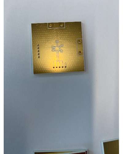
PCB RF (Circuiti stampati a radiofrequenza) sono circuiti stampati specializzati progettati per funzionare a radiofrequenze, tipicamente vanno da 3 kHz a 300 GHz. Questi PCB sono fondamentali nelle applicazioni che richiedono una trasmissione del segnale precisa ed efficiente con perdite e distorsioni minime. Questo articolo esplora le proprietà, struttura, materiali, processi di produzione, applicazioni, vantaggi, e domande frequenti (FAQ) relativi ai PCB RF.
Struttura dei PCB RF
La struttura dei PCB RF è meticolosamente progettata per supportare alta frequenza integrità e prestazioni del segnale:
Il substrato è tipicamente costituito da materiali con una costante dielettrica e una tangente di perdita basse, come il PTFE (politetrafluoroetilene), Laminati Rogers, o compositi PTFE riempiti con ceramica. Questi materiali aiutano a ridurre al minimo la perdita di segnale e garantiscono prestazioni stabili alle alte frequenze.
Per le tracce vengono utilizzati sottili strati di rame o altri metalli conduttivi, garantendo una perdita minima di segnale e prestazioni ad alta frequenza. Questi strati sono spesso incisi con precisione per formare gli schemi circuitali necessari.
Per separare gli strati conduttivi vengono utilizzati materiali dielettrici ad alte prestazioni, mantenendo l'isolamento elettrico e l'integrità del segnale. Questi strati sono fondamentali per prevenire l'interferenza del segnale e la diafonia tra tracce adiacenti.
I piani di massa dedicati forniscono un piano di riferimento per i segnali, riducendo le interferenze elettromagnetiche (EMI) e migliorare la qualità del segnale. Anche i piani di massa svolgono un ruolo fondamentale nella gestione termica dissipando il calore generato dalle operazioni ad alta frequenza.
Le interconnessioni verticali collegano diversi strati del PCB, consentendo percorsi complessi e progetti ad alta densità. Microvie, in particolare, sono utilizzati nell'interconnessione ad alta densità (ISU) progettazioni per ridurre al minimo l'induttanza e la capacità parassite.
Rivestimenti protettivi come ENIG (Oro per immersione in nichel chimico) o OSP (Conservanti organici di saldabilità) sono utilizzati per migliorare la saldabilità e proteggere dall'ossidazione. Queste finiture aiutano anche a garantire collegamenti elettrici affidabili.
Materiali utilizzati nei PCB RF
I materiali chiave utilizzati nei PCB RF includono:
Un materiale dielettrico a bassa perdita noto per le sue eccellenti prestazioni e stabilità alle alte frequenze. Il PTFE viene spesso utilizzato in applicazioni che richiedono un'attenuazione minima del segnale e un'elevata integrità del segnale.
Laminati ad alte prestazioni con costante dielettrica e tangente di perdita basse, specificatamente progettato per applicazioni RF e microonde. I materiali Rogers sono preferiti per le loro proprietà elettriche costanti e l'affidabilità alle alte frequenze.
Questi materiali offrono un equilibrio di bassa perdita, elevata conduttività termica, e stabilità meccanica. Sono spesso utilizzati in applicazioni in cui la gestione termica e la robustezza meccanica sono fondamentali.
Il rame di elevata purezza viene utilizzato per tracce conduttive grazie alla sua eccellente conduttività elettrica e affidabilità. La bassa resistenza del rame aiuta a mantenere l'integrità del segnale alle alte frequenze.
Materiali con costante dielettrica e tangente di perdita basse, come il Teflon (PTFE) e materiali Rogers specializzati, vengono utilizzati per garantire una perdita e una distorsione minime del segnale. Questi materiali sono fondamentali per mantenere un'elevata qualità del segnale.
Processo di produzione di PCB RF
Il processo di produzione dei PCB RF prevede diversi passaggi precisi per garantire prestazioni e affidabilità ad alta frequenza:
Scelta dei materiali di base e degli strati conduttivi appropriati in base ai requisiti prestazionali. Il processo di selezione considera fattori come la costante dielettrica, tangente di perdita, proprietà termiche, e resistenza meccanica.
Impilamento e incollaggio di più strati di materiali conduttivi e dielettrici in condizioni controllate per formare un PCB stabile. Questo processo garantisce uno spessore e un allineamento costanti dello strato.
Foratura di precisione per creare via e microvia per le interconnessioni verticali tra gli strati. Per le microvie vengono spesso utilizzate tecniche avanzate di perforazione laser per ottenere un'elevata precisione e danni minimi ai materiali circostanti.
Galvanotecnica del rame sul substrato e sui passaggi interni per stabilire connessioni elettriche affidabili. Questo passaggio garantisce vie forti e conduttive per la trasmissione del segnale.
Utilizzo della fotolitografia e dell'incisione chimica per definire i modelli di circuito e le interconnessioni. La modellazione precisa è essenziale per ottenere il layout e le prestazioni del circuito desiderati.
Applicazione di rivestimenti protettivi su superfici di rame esposte per migliorare la saldabilità e proteggere dall'ossidazione. Le finiture superficiali aiutano inoltre a prevenire la corrosione e garantiscono affidabilità a lungo termine.
Collegamento di componenti mediante tecniche di saldatura adatte per applicazioni ad alta frequenza, garantendo una perdita di segnale e una distorsione minime. Il processo di assemblaggio prevede un accurato posizionamento e saldatura dei componenti RF per mantenere l'integrità del segnale.
Test rigorosi per le prestazioni elettriche, Integrità del segnale, e rispetto delle specifiche di progettazione. I test includono misurazioni della perdita di segnale, controlli di impedenza, e cicli termici per garantire l'affidabilità in condizioni operative.
Applicazioni dei PCB RF
I PCB RF sono utilizzati in un'ampia gamma di applicazioni ad alta frequenza, tra cui:
Stazioni base, antenne, e moduli RF per reti di comunicazione mobile e wireless. I PCB RF sono essenziali per trasmettere e ricevere segnali ad alta frequenza nei sistemi di comunicazione.
Sistemi radar ad alta frequenza utilizzati nella difesa, aerospaziale, e applicazioni automobilistiche. I PCB RF consentono un'elaborazione e una trasmissione accurata del segnale nei sistemi radar.
Apparecchiature per la diagnostica e l'imaging, come macchine per risonanza magnetica e ultrasuoni, che richiedono l'elaborazione del segnale ad alta frequenza. I PCB RF garantiscono una trasmissione del segnale precisa e affidabile nei dispositivi medici.
Transponder, ricevitori, e trasmettitori utilizzati nei sistemi di comunicazione satellitare. I PCB RF supportano collegamenti di comunicazione ad alta frequenza nei sistemi satellitari.
Sensori e sistemi di controllo ad alta frequenza utilizzati negli ambienti di produzione e di controllo dei processi. I PCB RF consentono un'elaborazione del segnale affidabile ed efficiente nell'automazione industriale.
Vantaggi dei PCB RF
I PCB RF offrono numerosi vantaggi significativi:
Progettato per supportare le frequenze RF con perdita di segnale e distorsione minime. I PCB RF garantiscono un'elevata integrità del segnale e prestazioni alle alte frequenze.
Mantiene la qualità e l'integrità del segnale attraverso l'uso di materiali a bassa perdita e processi di produzione precisi. I PCB RF riducono al minimo l'attenuazione e le interferenze del segnale.
La struttura robusta e i test garantiscono prestazioni e affidabilità a lungo termine nelle impegnative applicazioni ad alta frequenza. I PCB RF sono costruiti per resistere a condizioni operative difficili.
Efficace dissipazione del calore attraverso i materiali del substrato e le caratteristiche del design, garantendo un funzionamento stabile in condizioni di alta potenza. I PCB RF prevengono il surriscaldamento e i danni termici.
Adatto per un'ampia gamma di applicazioni ad alta frequenza in vari settori. I PCB RF possono essere personalizzati per soddisfare specifici requisiti di progettazione e prestazioni.
Domande frequenti
Quali materiali vengono generalmente utilizzati per i PCB RF, e perché?
I PCB RF utilizzano comunemente materiali come il PTFE, Laminati Rogers, e compositi PTFE riempiti con ceramica per la loro bassa costante dielettrica, tangente a bassa perdita, e stabilità alle alte frequenze. Questi materiali sono essenziali per mantenere l'integrità e le prestazioni del segnale.
In che modo i PCB RF differiscono dai PCB standard?
I PCB RF sono progettati specificamente per applicazioni ad alta frequenza, utilizzando materiali e processi di produzione specializzati per ridurre al minimo la perdita e la distorsione del segnale. I PCB standard vengono generalmente utilizzati per applicazioni a frequenza più bassa e potrebbero non richiedere caratteristiche prestazionali così rigorose.
Quali settori traggono maggiori vantaggi dall'uso dei PCB RF?
Settori come le telecomunicazioni, aerospaziale e della difesa, dispositivi medici, comunicazioni satellitari, e l'automazione industriale traggono notevoli vantaggi dall'uso dei PCB RF grazie alle loro prestazioni e affidabilità ad alta frequenza.
Come vengono testati i PCB RF per garantirne l'affidabilità?
I PCB RF sono sottoposti a rigorosi processi di test, compresi test elettrici per l'integrità e le prestazioni del segnale, Ciclismo termico, e test di affidabilità. Questi test garantiscono che i PCB RF soddisfino rigorosi standard di prestazioni e durata ad alta frequenza.