株式会社")
半導体 BGA基板メーカー, 極小バンプピッチ基板を主に生産しております, 超小型のトレースと間隔 包装基板
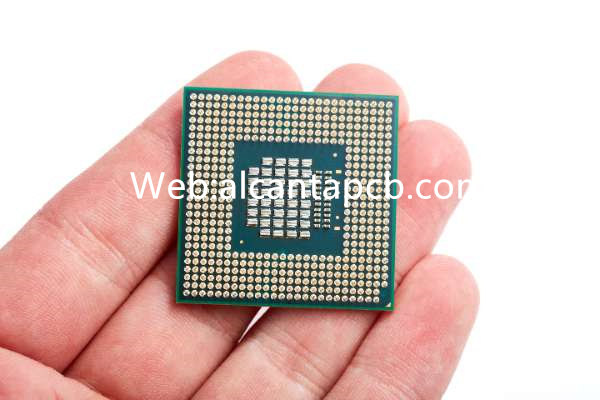
半導体BGA (ボールグリッドアレイ) 基板は、集積回路のパッケージングと接続に広く使用されている高密度パッケージング技術です。 (IC). 接続媒体として球状のはんだボールを使用します, 回路基板上のチップをこれらの球状のはんだボールを介してマザーボードまたは他のデバイスに接続できるようにします。. 従来のピンベースのパッケージングとの比較, BGA 基板は、より高い接続密度とより優れた電気的性能を実現できます。.
BGA基板は通常、半導体材料で作られています, シリコンなどの, ガリウムヒ素 (GaAs), 等. その構造はチップで構成されています, 包装基板, 球状はんだボールとコネクタ. 製造工程中, チップは基板上にパッケージされ、はんだ付け技術によって接続されます。. このパッケージング技術により、BGA 基板の信頼性と熱管理機能が向上します。, さまざまな高性能電子デバイスの用途に適しています。.
BGA 基板の主な特徴は次のとおりです。:
高密度接続: 球状はんだボール接続技術による, BGA 基板はより高密度の接続を実現できます, より多くのチップとデバイスを回路基板に搭載できるようになります.
優れた電気的性能: BGA基板は信号伝送経路が短く、抵抗とインダクタンスが小さい, これにより、回路のパフォーマンスと安定性が向上します。.
優れた熱管理: はんだボールと基板間の良好な接触により、, BGA 基板は、チップによって生成された熱をより効果的に伝達および分散できます。, チップの熱ストレスを軽減し、システムの信頼性を向上させます。.
一般的に, 半導体 BGA 基板は、電子機器の設計と製造に安定した高性能ソリューションを提供する高度なパッケージング技術です。. エレクトロニクス産業の継続的な発展と進歩に伴い、, BGA基板は今後も重要な役割を果たしていく, 技術の継続的な革新と用途の拡大を促進する.
半導体BGA基板の製造工程とは?
半導体 BGA 基板の製造プロセスには、複数の重要なステップが含まれます, 各ステップは非常に重要であり、最終製品の品質と性能に影響を与えます。. これらの主要な手順については、以下で詳しく説明します:
デザイン: 半導体BGA基板製造の最初のステップは設計です. この段階では, メーカーは顧客と協力して仕様を決定します, 寸法, そして基板のレイアウト. 設計チームは CAD ソフトウェアを使用して設計し、基板の配線とコネクタのレイアウトが製品要件を満たしていることを確認します。.
材料の選択: 特定の用途に適した高性能半導体材料を選択することは、製造プロセスにおける重要なステップです. これらの材料には基板材料が含まれます, 梱包材, 金属線, 等. メーカーは、基板の安定性と信頼性を確保するために、製品要件と性能指標に基づいて適切な材料を選択します。.
グラフィックスおよび画像処理: メーカーは、設計された BGA 基板イメージをグラフィックスおよび画像処理ソフトウェアにインポートします。, 最終的なイメージが設計要件を正確に反映できるように、さまざまなパラメーターの調整と最適化を実行します。.
フォトリソグラフィ: 製造工程中, フォトリソグラフィーは、設計されたパターンを基板表面に転写するために使用されます。. フォトリソグラフィーは、感光性樹脂とフォトレジストを使用して基板の表面にパターンを投影し、対応する化学処理を実行して目的のパターンを形成する精密なプロセスです。.
エッチング: フォトリソグラフィの後, 基板表面から材料の不要な部分を除去するにはエッチングプロセスが必要です, 必要なパターンとコネクタを残す. エッチングには化学エッチングや物理エッチングなどの方法を使用できます。, さまざまな材料や設計要件に応じて、適切なエッチングプロセスを選択できます。.
メタライゼーション: エッチング完了後, コネクタの導電性能を高めるために基板の表面を金属化する必要がある. メタライゼーションでは、電気めっきや化学蒸着などの方法を使用して、基板の表面に金属層を堆積し、導電性コネクタを形成できます。.
包装: パッケージングは、集積回路チップを BGA 基板に実装するプロセスです. メーカーは高度な機器を使用してチップを基板に接着し、はんだ付けまたはその他の固定方法で所定の位置に保持します。. パッケージングプロセスには、チップの安定性と放熱性能を高めるためのヒートシンクの取り付けやパッケージング接着剤の充填などのステップも含まれます。.
テストと品質管理: 最後の重要なステップは、製造された BGA 基板の厳格なテストと品質管理です。. メーカーはさまざまな試験装置や方法を使用して基板の性能を試験し、製品の要件や基準を満たしていることを確認します。. テストに合格した基板のみが顧客に納品され、使用できるようになります。.
総括する, 半導体 BGA 基板の製造プロセスには、設計などの複数の重要なステップが含まれます。, 材料の選択, グラフィックスと画像処理, フォトリソグラフィ, エッチング, 金属化, 梱包, テストと品質管理. 最終製品の品質と性能が顧客の要件と期待を確実に満たすために、各ステップには高度な機器と技術サポートが必要です。.
他の基板と比較した半導体BGA基板の利点は何ですか?
半導体 BGA 基板には他の基板に比べて多くの利点があります, そのため、今日のエレクトロニクス分野で好まれるパッケージング技術の 1 つとなっています。.
初め, 半導体BGA基板は高密度です. BGA基板はボールグリッドアレイ接続技術を採用. 従来の包装方法と比較して, 接続点がより密になっています, そのため、限られたスペースでより多くのコネクタとチップを収容できます. このため、BGA 基板は高密度集積回路設計の実装に最適です。, 特に小型電子機器や高性能アプリケーション向け.
第二に, BGA 基板は優れた電気的性能と信号伝送特性を備えています。. ボールグリッドアレイ接続技術の採用により, BGA 基板は信号経路を短くし、抵抗とインダクタンスを低くすることができます。, これにより、信号の遅延と損失が軽減されます。, 信号伝送の安定性と信頼性の向上. これは、高速データ伝送と低消費電力を必要とするアプリケーションにとって特に重要です。, 通信機器など, コンピューターと家庭用電化製品.
加えて, 半導体 BGA 基板は優れた熱管理特性を備えています. BGA 基板の設計により、チップから発生する熱をより効果的に分散および放散できます。, これによりシステム温度が低下し、放熱効率が向上します。. これは、システムの安定性と信頼性を確保するために、高性能チップや長時間稼働するデバイスにとって重要です。.
加えて, BGA基板は信頼性と耐衝撃性も向上. その溶接方法はより信頼性が高く、接続ポイントはボールグリッドによって基板の下にカプセル化されているためです。, 機械的衝撃や振動に対する耐性が向上します。, 外部環境要因による断線や損傷を軽減. これにより、BGA基板は産業用制御などの分野で広く使用されています。, 自動車エレクトロニクス, と航空宇宙, 機器の信頼性と耐久性に対する非常に高い要件が求められる場所.
総括する, 半導体BGA基板には高密度などの多くの利点があります, 優れた電気性能, 他の基板よりも優れた熱管理性能と高い信頼性を実現. これらの利点により、BGA 基板はさまざまな電子デバイスに推奨されるパッケージング ソリューションとなっています。, エレクトロニクス産業の継続的な発展と進歩を推進する.
半導体BGA基板はどのような分野で使われているのか?
半導体BGA基板は現代技術の分野で広く使用されており、さまざまな分野で重要な役割を果たしています. 以下は、半導体 BGA 基板アプリケーションのいくつかの主要分野です。:
電子通信の分野では, 半導体BGA基板は携帯電話に広く使用されています, 衛星通信設備, 通信基地局およびその他の機器. 高密度接続と高性能特性により, BGA 基板は複雑な通信システムをサポートし、通信機器の性能と信頼性を向上させることができます。.
半導体BGA基板はコンピュータやネットワーク機器にも広く使用されています, パソコンも含めて, サーバー, ルーター, スイッチ, 等. BGA 基板は安定した回路接続とパッケージング ソリューションを提供します, コンピュータやネットワーク機器の高速動作をサポート.
カーエレクトロニクス分野では, 半導体BGA基板は自動車の電子制御システムに使用されます, 車載エンターテイメントシステム, ナビゲーションシステム, 等. BGA 基板は自動車の作業環境の課題に耐えることができ、高い耐熱性と耐衝撃性を備えています。, 車載電子機器の安定性と信頼性の確保.
半導体BGA基板は医療機器でも重要な役割を果たしています, 医療診断機器を含む, 監視装置, 医療イメージング機器, 等. BGA 基板は正確な回路接続とパッケージングのソリューションを提供します, 医療機器の精度と信頼性を確保し、医療業界の発展に貢献します.
産業自動化の分野で, FA機器に使用される半導体BGA基板, ロボットシステム, センサー制御システム, 等. BGA 基板は高密度接続と高性能を特徴とします, 複雑な産業オートメーションシステムをサポートし、生産効率と製品品質を向上させることができます。.
一般的に, 半導体BGA基板は電子通信で広く使用されています, コンピュータおよびネットワーク機器, 自動車エレクトロニクス, 医療機器, 産業用自動化およびその他の分野. 高性能・高信頼性により、さまざまな分野の機器に安定かつ効率的な回路接続および実装ソリューションを提供します。, 現代技術の開発と進歩を促進する.
適切な半導体 BGA 基板メーカーを見つける方法?
適切な半導体 BGA 基板メーカーを見つけるには, 次の要素を考慮する必要があります:
技術的能力: 初め, メーカーの技術力を評価する必要がある. これには設計能力も含まれます, 製造工程, と品質管理システム. 製品のニーズを満たすのに十分な経験と専門知識を持っていることを確認してください.
生産能力: メーカーの生産能力も重要な要素です. 注文のニーズを満たすのに十分な生産設備と人材を確保する必要があります。, 高品質の製品を納期通りに納品できることはもちろんのこと、.
品質基準: 品質はメーカーを選択する際の重要な考慮事項の 1 つです. メーカーが国際規格と業界認証に準拠していることを確認する, ISOなど 9001 品質マネジメントシステム認証, および顧客が必要とするその他の証明書.
費用対効果: 品質に加えて, 費用対効果も考慮事項の1つです. メーカーの価格が妥当かどうかを評価し、他の競合他社と比較する必要があります. ただし、低価格を選択すると、製品の品質やサービス レベルに影響が出る可能性があることに注意してください。.
サプライチェーンの信頼性: メーカーのサプライチェーンの信頼性も重要な考慮事項です. 生産スケジュールに影響を与えないよう、サプライチェーンが安定しており、必要な原材料をタイムリーに供給できることを確認してください。.
サービスとサポート: ついに, メーカーが提供するサービスやサポートも考慮したい. これには技術サポートが含まれます, アフターサービス, 顧客とコミュニケーションし、協力する能力. 充実したサポートを提供できるメーカーを選ぶ, 生産プロセス中に発生した問題の解決に役立ちます, カスタマイズされたソリューションを提供します.
総括する, 適切な半導体 BGA 基板メーカーを見つけるには、技術力などの要素を総合的に考慮する必要があります。, 生産能力, 品質基準, 費用対効果, サプライチェーンの信頼性, サービスとサポート. これらの要素を慎重に評価し、サプライヤーと十分にコミュニケーションを取り、協力することで、, あなたの会社のニーズに最適なメーカーを見つけることができます.
半導体BGA基板のお見積り方法?
半導体 BGA 基板の見積もりを取得することは重要なステップです, ただし、最終的に適切なサプライヤーと製品を確実に選択するために、このプロセスを実行する際に注意すべき重要な問題がいくつかあります。. 考慮すべき点がいくつかあります:
業者に見積もりを依頼する前に, プロジェクトの完全な仕様が明確であることを確認してください. これにはサイズに関する詳細な要件が含まれます, 材料, レイヤー数, 表面処理, 絞りサイズ, 線幅と行間, 等. 明確な仕様を提供することで、サプライヤーはお客様が何を必要としているのかを正確に理解し、それに応じて見積もることができます。.
必要な BGA 基板の体積要件を決定することが非常に重要です. 一般的に言えば, 注文数量が多いほど、より競争力のある価格が得られます. したがって, サプライヤーに問い合わせる際には、正確な推定注文数量を提供することが非常に必要です.
サプライヤーのリードタイムと生産リードタイムを理解することも重要です. サプライヤーによって生産サイクルが異なる場合があります, これはプロジェクトの進行に直接影響します. したがって, サプライヤーを選ぶとき, 生産能力と、時間要件を満たせるかどうかを考慮する必要があります。.
選択したサプライヤーが優れた品質保証システムと関連認証を備えていることを確認します。. 例えば, ISO 9001 品質マネジメントシステム認証, 等. これにより、購入した BGA 基板が信頼できる品質であることを確認できます。, 安定していて信頼できる.
価格や品質だけでなく、, サプライヤーのサービスとサポートも同様に重要です. これには技術サポートが含まれます, アフターサービス, 問題に迅速に対応する能力. サプライヤーを選ぶとき, サービスレベルを考慮することが重要です.
サプライヤーから提供される見積もりが明確かつ透明であることを確認してください, すべての費用の詳細な説明を含む. これにより、見積書の各費用の出所をより深く理解し、より正確な比較と評価を行うことができます。.
一般的に, 半導体BGA基板の見積りは価格を総合的に考慮する必要があります, 品質, 納期, サービスサポートなど. 十分な理解とコミュニケーションを通じて, 適切なサプライヤーを選択することで、プロジェクトに安定した信頼性の高い基板ソリューションを提供できます。.
よくある質問
半導体BGA基板とは?
半導体BGA基板, ボールグリッドアレイ基板としても知られています, 電子機器に欠かせない部品です, 集積回路のパッケージングと相互接続を容易にする. これらの基板は、高密度の相互接続機能と優れた電気的性能を提供します。.
半導体BGA基板メーカーはどのような役割を果たしているのか?
半導体BGA基板メーカーが設計を担当, 生産する, 電子デバイスの仕様と要件を満たすためにこれらの基板をテストします. 信頼性を確保します, パフォーマンス, 高度な製造プロセスと品質管理手段による BGA 基板の品質と品質.
半導体BGA基板はどのように製造されるのか?
半導体 BGA 基板の製造プロセスには、いくつかの重要なステップが含まれます, デザインも含めて, 材料の選択, 処理, 梱包, およびテスト. 高度な技術と設備を利用して、正確な寸法の基板を製造します, 構造物, および電気的特性.
半導体 BGA 基板が他の基板に比べて提供する利点は何ですか?
半導体 BGA 基板にはいくつかの利点があります, 高密度相互接続を含む, 電気性能の向上, 熱管理の改善, 優れた信頼性. これらの基板により、電子デバイスへの複雑な回路設計の統合が可能になります。, 機能と性能に貢献する.
半導体BGA基板はどのような用途に一般的に使用されていますか?
半導体 BGA 基板はさまざまな電子機器に広く応用されています, スマートフォンを含む, 錠剤, コンピュータ, 自動車エレクトロニクス, などなど. これらは、これらのデバイスの集積回路をパッケージングおよび接続するための重要なコンポーネントとして機能します。, 機能とパフォーマンスをサポートする.