株式会社")
私たちは半導体パッケージング用基板のプロフェッショナルです, 極小バンプピッチ基板を主に生産しております, 超小型のトレースと間隔 包装基板 そして プリント基板.
今日のデジタル時代では, 半導体技術の急速な発展は、電子機器の継続的な革新を推進します. この素晴らしいテクノロジーの裏側には, 半導体パッケージングの役割はますます重要になっています. 包装システム全体で, 基板, 欠かせない要素として, 重要な役割を果たしています.
半導体基板は電子機器を支えるシステムです. 建物の礎石のように機能し、チップの安定したプラットフォームを提供します. 基板にはチップとそれに接続されたさまざまなコンポーネントが搭載されています, 同時にこれらのコンポーネントを回路を通じて接続して完全なパッケージ構造を形成します. その性能, 電子製品では安定性と信頼性が極めて重要です.
基板の材料選択と設計は、熱管理に直接影響します。, パッケージの電気的性能と全体的な信頼性. 電子部品を機械的にサポートするだけではありません, 複雑な回路接続を通じて機器の正常な動作も保証します。.
この記事では、半導体パッケージ基板について包括的に説明します。, 彼らの基本的な特徴を掘り下げる, 多様なタイプ, さまざまな業界にわたるアプリケーション. 基板の技術基盤を精査します, 電子機器の製造におけるそれらの複雑な役割を解明する. 材料選択の基本から高度なリジッドフレックスボード技術の複雑さまで, 基板の進化の旅をたどります パッケージングテクノロジー 技術開発の将来の動向を予測する. 基板の複雑さに没頭することで, 私たちはエレクトロニクス市場の進化するニーズをよりよく理解し、それに対処することを目指しています, イノベーションと持続可能性によって特徴付けられる未来に向けて業界を推進する.
半導体パッケージングにおける基板の役割
半導体パッケージング分野では, 下地は重要な役割を果たします, そしてその定義と機能は、一般的な材料のサポートをはるかに超えています。. 半導体パッケージングにおける基板の複数の役割を詳しく見てみましょう.
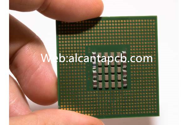
半導体パッケージの基板は重要な部品です, 通常は導電性材料で作られています, チップをサポートし接続する. その特別な設計は、電子機器の複雑なニーズを満たすように設計されています。, それにより、半導体パッケージングにおいて独自の役割を果たします.
チップを保護する: 基板はパッケージングプロセス中にチップの保護層として機能します。, チップに対する外部環境の悪影響を効果的に隔離します。, 湿気などの, 粉塵や化学物質. これにより、チップの長期安定動作が保証されます。.
サポート構造: 基板はチップの構造支持体として機能します, 外部応力を分散および吸収し、包装システム全体の構造強度を向上させるのに役立ちます。. これは、衝撃や振動に対するデバイスの耐性を向上させるために重要です。.
電気接続: 基板は、その導電層を介してチップに重要な電気接続を提供します。. この接続により、チップが外部回路と通信できるようになるだけではありません。, だけでなく、チップが設計仕様内で動作することを保証するために電流と電圧を調整するのにも役立ちます.
放熱機能: 熱伝導性に優れた材料で作られた基板は、チップから発生する熱を効果的に放散し、チップの動作を適切な温度範囲に維持します。. これはデバイスのパフォーマンスと寿命を向上させるために非常に重要です.
半導体パッケージで, 基板は単なる支持材料ではありません, 多機能な主要コンポーネントでもあります. 保護する複数の機能, チップのサポートと接続により、パッケージング システムの信頼性と安定性が確保されます。. 基板の精密設計と材料選択は、将来の半導体技術開発においてますます重要な役割を果たします, エレクトロニクス業界をより高いパフォーマンスと持続可能性に向けて推進.
半導体パッケージ基板の主な特徴
半導体パッケージで, 基板はシステム全体のサポートおよび重要なコンポーネントです. 半導体パッケージ基板の主な特性を理解することは、電子デバイスの性能と信頼性を確保するために重要です。. 下地の主な特徴を詳しく見てみましょう:
半導体パッケージ基板の性能は材料の選択に直接影響されます。. 一般的な基板材料には FR-4 が含まれます, 金属基板とセラミックス. FR-4 は、優れた絶縁特性と機械的強度を備え、広く使用されているガラス繊維強化エポキシ樹脂基板です。. 488さまざまな材料の特性を理解し、適切な基板材料を選択することは、半導体パッケージングにとって重要です。.
半導体デバイスは動作中に発熱します。, 効果的な熱管理は、システムのパフォーマンスと寿命を確保するための重要な要素です。. 基板は、効果的に熱処理を行うことでこのプロセスにおいて重要な役割を果たします。, 発生した熱を分散、放散する. 熱伝導率の良い基板材料を使用, 適切に設計された放熱構造, 効果的な放熱ソリューションはすべて、半導体デバイスの安定した動作を確保するために重要な考慮事項です。.
半導体パッケージ基板は回路の電気的性能に直接影響します。. 基板の電気特性には誘電率が含まれます。, 損失係数, インピーダンスマッチング, 等. これらのパラメータは信号伝送の品質と速度に直接関係します。. 適切な基板材料の選択と適切な配線構造の設計により、, 信号の減衰と歪みを最小限に抑えることができ、回路の全体的なパフォーマンスが向上します。.
材料を包括する極めて重要な特性を考慮する, デザイン, そして選択, 半導体パッケージ基板を設計する戦略的プロセスが重要な鍵として浮上. このプロセスはシステムの信頼性を保証するのに役立ちます, 優れたパフォーマンス, さまざまなアプリケーションの多様な要求に応える能力. これは、材料科学および材料工学の領域における設計上の課題であるだけでなく、進化し続けるエレクトロニクス業界での勝利の決定的な要素でもあります。.
半導体パッケージ基板の種類
半導体パッケージングの領域内, 多様な基質が豊富にある, それぞれが独自の特性とカスタマイズされた用途を誇ります. 電子機器のパフォーマンスを最適化するためには、これらのカテゴリを微妙に理解することが不可欠であることがわかります。.
BGAパッケージ基板 (ボールグリッドアレイ)
BGA パッケージ基板はボール グリッド アレイ パッケージであり、チップの底部が小さな球状のはんだ接合で覆われているという点で独特です。. この設計により、接続密度が高まり、信号伝送経路が短くなります。, これにより回路性能が向上します. BGA 基板は高性能コンピューティングおよび通信機器で広く使用されています, 電子製品に優れた信頼性と性能を提供します.
HDIテクノロジー (高密度相互接続)
HDI技術は、基板上にミクロン単位の配線を実現し、電子部品間の接続密度を高める高密度配線技術です。. この技術により、より多くのコンポーネントをより小さなスペースに統合できるようになります。, 電子機器の小型・軽量化の条件を整える. HDI基板はスマートフォンやラップトップなどのポータブル機器で重要な役割を果たします.
リジッドフレキシブル基板
リジッドフレックス基板は、リジッド基板とフレキシブル基板の特性を組み合わせた設計です。. リジッド基板とフレキシブル基板を貼り合わせることで、さまざまな環境やストレスへの適応性を実現. リジッドフレックスボードは軍事分野で広く使用されています, 医療および自動車エレクトロニクス, 高統合性と優れた耐久性の両方の要件を満たすことができるため、好まれています。.
これらのさまざまなタイプの半導体パッケージ基板は、エレクトロニクス業界が柔軟性を追求し続けていることを示しています。, 高性能, と信頼性. これらのカテゴリを深く理解することは、電子製品の設計を最適化し、業界の継続的な革新と開発を促進するのに役立ちます。.
半導体パッケージ基板応用分野
半導体パッケージ基板, 電子機器の主要部品として, さまざまな分野で広く使用されています, さまざまなアプリケーション シナリオに対して強力なサポートとパフォーマンスの最適化を提供します。. 以下は、3 つの主要分野における半導体パッケージ基板の詳細な用途です。:
電子機器の製造に欠かせない半導体パッケージ基板, 二重の役割を果たす. まず最初に, チップの堅牢なサポートおよび接続プラットフォームとして機能します。, 高密度配線技術により確実な電気接続を実現. この側面は、一連の電子製品の堅牢な性能基盤を形成します。, スマートフォンを含む, 錠剤, そしてラップトップ. 第二に, 基板の熱管理特性により、高性能電子デバイスに特に適しています。, 長期間の動作期間中に安定した温度を確保.
高密度配線技術の採用により, 基板は通信機器の回路レイアウトをコンパクトにします。, 高速信号伝送と効率的なデータ処理をサポート. ネットワーク機器内かどうか, 無線通信モジュールまたは衛星通信システム, 基板は装置の安定稼働に重要な役割を果たします。.
車載電子システムの進歩は、半導体パッケージ基板のサポートと切り離すことができません。. 自動車における基板の用途は、車載エンターテイメント システムに限定されません, ただし、エンジン制御ユニットなどの重要な領域も含まれます, 車両安全システム, そして自動運転技術. リジッドフレキシブル基板の設計により、基板は自動車の複雑な作業環境に適応できます。, 信頼性の高い接続を提供しながら、車両電子システムの正常な動作を保証します。.
これら 3 つの主要な分野では, 半導体パッケージ基板はその多用途性と適応性を実証します, さまざまなアプリケーション シナリオに重要なサポートを提供する. エレクトロニクス業界が革新を続けているにつれて, 基板は今後も様々な分野で技術開発や製品の性能向上を推進する中心的な役割を果たしていきます. これは基板技術だけの勝利ではありません, エレクトロニクス分野における継続的な革新の鮮やかな現れでもあります.
半導体パッケージ基板の今後の動向
半導体パッケージ基板技術はエキサイティングな発展期を迎えています, そして将来の傾向は次の主要分野に焦点を当てます。:
材料研究の進歩: 進化を続ける半導体業界では、新しい材料に対する需要が高まっています. 基板メーカーは、軽くて強いだけでなく、導電性も向上した材料の開発に積極的に取り組んでいます。. この追求は、基板の性能を向上させ、電子デバイスへの適用範囲を広げることを目的としています。.
高密度相互接続テクノロジー: 電子機器のサイズは縮小しつつも出力は増大するため、, 基板上の高密度相互接続のニーズが高まっています. 基板設計の将来の軌道は、複雑な回路の要求に応えるためにより多くの接続ポイントを実現することに重点が置かれることによって特徴づけられるでしょう。.
最先端の放熱技術: チップのパワーの増大と並行して, 効果的な熱放散が最も重要になってきています. 将来の基板設計では、放熱効率の向上に重点が置かれることになる, 電子機器の安定動作を確保するための革新的な素材と構造を採用.
ますます深刻化する環境課題に直面して, 半導体パッケージ基板メーカーは持続可能性と環境保護にますます注力するようになる. 今後のトレンドとしては、:
グリーンマテリアルの採用: 基板メーカーは、限られた資源への依存を減らし、環境への影響を減らすために、再生可能で分解可能な材料を使用する傾向があります。.
エネルギー効率の最適化: よりエネルギー効率の高い基板を設計して電子デバイスのエネルギー消費を削減する. 回路レイアウトと材料の選択を最適化してエネルギー効率を向上させ、世界的な持続可能性の目標を達成します.
循環経済の実践: 廃棄された電子機器のリサイクル性を重視. 将来の基板設計は循環経済の原則にさらに重点を置くことになる, リサイクルと再利用により廃棄物の発生を削減.
総合します, 半導体パッケージ基板の将来は、環境への負担を軽減するよう努めながら、成長するエレクトロニクス市場のニーズを満たすための技術革新と持続可能性に焦点が当てられます。. この発展傾向は半導体産業の進歩を促進するだけではありません, 社会のために、より持続可能で環境に優しい電子製品を生み出すこともできます。.