株式会社")
超薄型5G基板メーカー。超薄型5Gの先進企業として 基板 メーカー, 当社は次世代の高速通信向けに設計された最先端の基板の製造を専門としています。. 当社の超薄型基板は優れた信号整合性を提供します, 強化された熱管理, 並外れた信頼性, 5Gテクノロジーの厳しい要求に応える. 革新性と品質を重視, 高性能デバイスを実現する基板をお届けします, 急速に進化する 5G 環境においてシームレスな接続と最適なパフォーマンスを確保.
5Gテクノロジーの出現は通信に革命をもたらしました, 前例のないデータ速度を約束します, 超低遅延, そして大規模な接続性. これらの厳しい要件を満たすために, 5Gデバイスに使用される基板は高度な性能が必要です. 超薄型 5G 基板は、これらの最先端のアプリケーションをサポートするように設計されています, 高いパフォーマンスを提供する, 優れた信号の完全性, コンパクトなフォームファクターでの効率的な熱管理. この記事ではその機能について説明します, 設計上の考慮事項, 材料, 製造工程, アプリケーション, 超薄型5G基板の利点と.
超薄型5G基板とは?
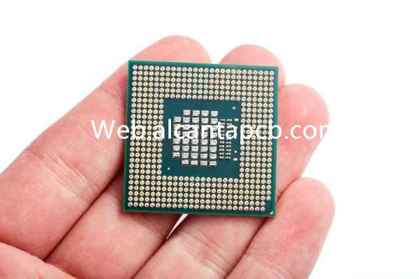
超薄型 5G 基板はプリント基板の一種です (プリント基板) 5G テクノロジーの高周波および高速要求をサポートするために特別に設計された材料. これらの基板の特徴は、最小限の厚さです。, 高い熱伝導率, 優れた電気的特性, 5G デバイスやインフラストラクチャへの統合に最適です. 超薄型プロファイルにより、コンパクトで軽量な設計が可能になります。, これらは現代の通信デバイスにとって重要です.
超薄型5G基板の特徴
超薄型 5G 基板には、高性能アプリケーションに適したいくつかの重要な特性があります。:
これらの基板は、5G 信号に関連する高周波を処理するように設計されています。, 最小限の信号損失と優れた伝送品質を確保.
高速電子部品から発生する熱を放散するには、効果的な熱伝導率が重要です。, 安定した動作温度を維持し、過熱を防ぎます。.
超薄型プロファイルにより、ある程度の柔軟性が得られます。, これは、性能を損なうことなく基板を曲げたり曲げたりする必要がある用途に有益です。.
薄さにもかかわらず, これらの基材は寸法安定性を維持します, 製造中および操作中にコンポーネントの正確な位置合わせと配置を保証する.
高純度の材料を使用することで欠陥や不純物を最小限に抑えます, 5G デバイスのパフォーマンスに影響を与える可能性があります.
超薄型 5G 基板の設計上の考慮事項
超薄型 5G 基板の設計には、最適なパフォーマンスと信頼性を確保するためにいくつかの重要な考慮事項が含まれます:
基板材料の選択は重要です. 液晶ポリマーなどの材料 (LCP), ポリテトラフルオロエチレン (PTFE), およびその他の高性能ポリマーは、その優れた電気的および熱的特性により一般的に使用されています。.
過熱を防ぐには効率的な熱管理が不可欠です. 設計には熱放散のための規定を含める必要があります, サーマルビアやヒートスプレッダーなど.
高周波での信号の完全性を維持することが重要です. これには配線インピーダンスの正確な制御が含まれます, 信号干渉を最小限に抑える, 効果的なシールド技術の導入.
基板は、製造プロセスや動作条件のストレスに耐えられる適切な機械的強度と柔軟性を備えていなければなりません。.
コンポーネントの適切な接着と位置合わせを確保するには、表面仕上げが滑らかで欠陥がない必要があります。.
超薄型5G基板に使用される材料
超薄型 5G 基板の製造にはいくつかの材料が一般的に使用されます:
LCPは優れた電気特性で知られています, 高い熱安定性, そして吸湿性が低い, 高周波アプリケーションに最適です.
PTFE は電気絶縁性と耐熱性に優れています。, RF およびマイクロ波アプリケーションで人気のある選択肢となっています。.
ポリイミド基板は優れた熱安定性と機械的柔軟性を提供します, 曲げや曲げが必要な用途に適しています.
先進的なセラミック素材, アルミナ、窒化アルミニウムなど, 高い熱伝導性と優れた電気絶縁性を実現, 高出力アプリケーションに適したものにする.
透明性と絶縁性を高めるためにガラス基板が使用されます。, 特に光電子デバイスにおいて.
超薄型5G基板の製造プロセス
超薄型 5G 基板の製造プロセスには、高品質とパフォーマンスを確保するためのいくつかの正確なステップが含まれます:
原料を準備し、所定のサイズにカットします. ポリマー基板用, これには、材料を薄いシートに押し出すか鋳造することが含まれます.
基板材料の複数の層を積層して、所望の厚さと特性を実現することができます。. このプロセスでは、層を接着するために熱と圧力がかかります。.
回路パターンはフォトリソグラフィープロセスを使用して作成されます. 感光性フィルム (フォトレジスト) 基材に適用されます, 紫外線にさらされる (紫外線) マスクを通した光, 目的の回路パターンを明らかにするために開発されました. 次に、基板をエッチングして不要な材料を除去します。.
基板にビアが開けられ、異なる層間に垂直方向の電気接続が形成されます。. これらの穴は銅でメッキされ、導電経路が確立されます。.
無電解ニッケル浸漬金などの表面仕上げ (同意する) はんだ付け性を高め、酸化から保護するために、接触パッドに浸漬銀が適用されます。.
最終基板は組み立てられる, コンポーネントが追加される場所. 厳格なテスト, シグナルインテグリティテストを含む, インピーダンスマッチングテスト, および環境ストレス試験, 基材が性能基準を満たしていることを確認するために実施されます.
超薄型5G基板の応用
超薄型 5G 基板はさまざまな高性能アプリケーションで使用されています:
これらの基板は高密度の製造に不可欠です, 最新のスマートフォンやタブレットで使用される高性能 PCB, より速いデータ速度と接続の改善を有効にします.
超薄型基板は、信頼性の高い信号の送受信に必要な高周波 RF コンポーネントをサポートするために 5G 基地局で使用されています。.
超薄型基板の柔軟性とコンパクトさはウェアラブルデバイスに最適です, 軽量で耐久性のある電子部品が必要な場合.
自動車業界では, これらの基板は先進運転支援システムで使用されています (ADAS) およびその他の高性能電子システム.
高速処理と信頼性の高い性能が求められる医療機器には極薄基板が採用されています, 画像診断システムや高度な監視装置など.
超薄型5G基板のメリット
超薄型 5G 基板には、高性能アプリケーションに欠かせないいくつかの利点があります。:
これらの基板は、5G 信号に関連する高周波を処理するように設計されています。, 最小限の信号損失と優れた伝送品質を確保.
レイヤードデザインにより効率的な熱放散が促進されます。, 過熱を防ぎ、安定した動作を保証します.
超薄型プロファイルにより、ある程度の柔軟性が得られます。, 性能を損なうことなく曲げや屈曲が必要な用途に有益.
これらの基板の厚さを薄くすることで、よりコンパクトで軽量な設計が可能になります。, これらは現代の通信デバイスにとって重要です.
高純度の材料を使用することで欠陥や不純物を最小限に抑えます, 5G デバイスの信頼できるパフォーマンスを確保する.
よくある質問
超薄型 5G 基板を使用する主な利点は何ですか?
主な利点としては、高周波性能が挙げられます。, 効率的な熱管理, 機械的柔軟性, コンパクトで軽量なデザイン, 高純度の材料を使用することにより、, 高速アプリケーションで信頼性の高いパフォーマンスを保証.
超薄型 5G 基板の製造に一般的に使用される材料は何ですか?
一般的な材料には液晶ポリマーが含まれます (LCP), ポリテトラフルオロエチレン (PTFE), ポリイミド, 先進的なセラミックス, そしてガラス. これらの材料は、優れた電気的および熱的特性を理由に選択されています。.
超薄型 5G 基板の設計により信号の完全性がどのように確保されるのか?
制御されたインピーダンスを提供することで信号の完全性を保証する設計, 信号干渉を最小限に抑える, 効果的なシールド技術の導入. シミュレーション ツールは、高周波パフォーマンスのこれらの側面を最適化するために使用されます。.
超薄型 5G 基板の一般的な用途は何ですか?
一般的なアプリケーションにはスマートフォンやタブレットが含まれます, 5G基地局, ウェアラブルデバイス, 自動車エレクトロニクス, および医療機器. これらの基板は、高密度の相互接続と信頼性の高いパフォーマンスを必要とするシステムで使用されます。.