株式会社")
極薄 BGA基板 メーカー。当社は極薄BGA基板の大手メーカーです。, 高性能の生産に特化, 高度な電子アプリケーション向けの小型ソリューション. 当社の最先端の製造プロセスにより、優れた品質と信頼性が保証されます。, 電気通信などの業界における最新テクノロジーの要求に応える, コンピューティング, およびコンシューマーエレクトロニクス.
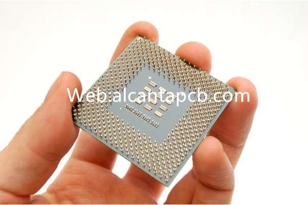
極薄ボールグリッドアレイ (BGA) 基板 集積回路のパッケージングに不可欠なコンポーネントです (IC), 特に高密度および高性能のアプリケーションにおいて. これらの基板は、電子パッケージ全体のサイズと重量を最小限に抑えながら、優れた電気的および熱的性能を提供します。. 極薄 BGA 基板は先端エレクトロニクスでますます使用されています, スマートフォンなどの, ラップトップ, およびその他のポータブルデバイス, スペースとパフォーマンスが重要な考慮事項となる場合.
超薄型BGA基板とは?
超薄型 BGA 基板は、半導体デバイスのパッケージングに使用される基板の一種です。. 半導体ダイを取り付けるベースとして機能し、ダイとプリント基板の間に必要な電気接続を提供します。 (プリント基板). の “極薄” 「側面」とは、従来の BGA 基板と比較して基板の厚さが減少していることを指します。, 電子パッケージの小型化と軽量化を実現.
BGA パッケージングでは、基板の底面にはんだボールを格子状に配置します。, リフローはんだ付けプロセス中に PCB への電気接続を作成するために使用されます。. 極薄 BGA 基板は同じ機能を維持しながら厚みを削減します, スペースが貴重な用途に最適です。.
超薄型 BGA 基板設計リファレンス ガイド
超薄型 BGA 基板の設計には、最適なパフォーマンスと信頼性を確保するためにいくつかの重要な考慮事項が含まれます. 次のセクションでは、超薄型 BGA 基板設計の重要な側面について概説します。.
設計段階では、いくつかの重要な考慮事項に対処する必要があります:
インピーダンス制御: 高周波での信号の完全性を維持するには、正確なインピーダンス制御が不可欠です. これには、信号トレースの慎重な設計と、制御されたインピーダンス材料の使用が含まれます。.
熱管理: 高出力アプリケーションには効果的な熱管理が重要です. 設計にはサーマルビアを組み込む必要があります, ヒートシンク, または熱を効率的に放散するためのその他の技術.
機械的安定性: 基板は、動作中の熱サイクルや機械的ストレスに耐えられるように、堅牢な機械的サポートを提供する必要があります。.
信頼性: 高品質の材料と精密な製造プロセスの使用により長期信頼性が保証されます。, 剥離や反りなどの問題を防止.
超薄型 BGA 基板に使用されている材料?
極薄 BGA 基板に使用される材料は、基板の全体的なパフォーマンスを向上させるために、相互に補完的な特性を考慮して選択されています。:
高性能ラミネート: 薄いプロファイルを維持しながら機械的強度と熱安定性を提供します. 一般的な材料にはポリイミドが含まれます, 液晶ポリマー (LCP), および高温FR-4.
極薄銅箔: 導電層に使用, 優れた導電性と信頼性を提供します.
低損失誘電体: 導電性トレースを絶縁し、信号の整合性を維持するために使用されます。.
高度な接着剤: 層を結合して機械的安定性を提供します.
極薄BGA基板のサイズはどれくらいですか?
超薄型 BGA 基板のサイズは、アプリケーションや特定の設計要件によって異なります。:
厚さ: 極薄 BGA 基板の厚さは通常、次の範囲です。 50 に 200 マイクロメートル, 設計とアプリケーションの要件に応じて.
寸法: 基板の長さと幅は、半導体ダイのサイズとシステムのレイアウトによって決まります。. 小型デバイス用の小さなフォームファクタから、より複雑な電子システム用の大型基板まで多岐にわたります。.
極薄BGA基板の製造プロセス
極薄 BGA 基板の製造プロセスには、高品質とパフォーマンスを確保するために正確に制御されたいくつかのステップが含まれます:
高品質ラミネート, 銅箔, 接着剤が選択され、加工のために準備されます. 材料は、不純物を除去し、滑らかな表面を確保するために洗浄および処理されます.
基板の層は熱と圧力を使用して貼り合わされます。. このステップにより、層が確実に接着され、基板の薄いプロファイルが維持されます。.
導電層はパターン化およびエッチングされ、必要な電気経路が作成されます。. これには、フォトリソグラフィーと化学エッチング技術を使用して、正確かつ正確なパターンを実現することが含まれます。.
基板に穴を開け、層間の電気接続のためのビアを作成します。. その後、ビアは銅でメッキされ、信頼性の高い導電性が確保されます。.
はんだボールは基板の下面に格子状に配置されています. これらのボールは、リフローはんだ付けプロセス中に PCB への電気接続を作成するために使用されます。.
製造後, 基板は、半導体ダイおよび必要なコンポーネントおよびコネクタと組み立てられます。. 基板がすべての設計仕様と性能要件を満たしていることを確認するために、厳格なテストが実施されます。. これには電気的性能のテストが含まれます, 熱管理, 機械的完全性.
極薄BGA基板の応用分野
超薄型 BGA 基板は、幅広い高性能アプリケーションで使用されています:
スマートフォンやタブレットなどのモバイル端末では, 超薄型 BGA 基板は、デバイス全体の厚さを最小限に抑えながら、高度な機能をサポートするために必要なパフォーマンスとコンパクトなサイズを提供します。.
ウェアラブルエレクトロニクスにおいて, 超薄型 BGA 基板により、コンパクトで軽量なフォームファクタに高度な機能を統合できます, 着用者の快適さと使いやすさを確保する.
ハイパフォーマンス コンピューティング アプリケーションにおいて, 超薄型 BGA 基板は、最新の CPU および GPU の高度な処理能力をサポートするために必要な電気的および熱的性能を提供します。.
通信機器において, 超薄型 BGA 基板は、高度な通信システムの高周波および高電力要件をサポートするために使用されます。.
自動車エレクトロニクス分野, 超薄型 BGA 基板は、高度な運転支援システムに必要な信頼性とパフォーマンスを提供します (ADAS) および車両内のその他の電子システム.
超薄型 BGA 基板の利点は何ですか?
超薄型 BGA 基板には、高性能アプリケーションに欠かせないいくつかの利点があります。:
コンパクトサイズ: 超薄型 BGA 基板により、コンパクトで軽量な電子パッケージの設計が可能になります, ポータブルおよびスペースに制約のあるアプリケーションに最適.
高い電気性能: 超薄型 BGA 基板は、信号損失を最小限に抑え、高い信号整合性を備えた優れた電気的性能を提供します。.
効率的な熱管理: 極薄 BGA 基板により効率的な熱管理が実現, 熱を効果的に放散し、高出力コンポーネントのパフォーマンスを維持します。.
機械的安定性: 極薄の BGA 基板が堅牢な機械的サポートを提供, 動作中の熱サイクルと機械的ストレスに耐える.
多用途性: 極薄BGA基板は幅広い用途に使用可能, モバイルデバイスからハイパフォーマンスコンピューティング、自動車エレクトロニクスまで.
よくある質問
超薄型 BGA 基板を設計する際の重要な考慮事項は何ですか??
主な考慮事項には、熱的および電気的性能のための材料の選択が含まれます, シグナルインテグリティと熱管理のためのレイヤースタックアップ, 機械的な安定性と信頼性を確保する.
超薄型 BGA 基板は従来の BGA 基板とどう違うのか?
超薄型 BGA 基板は、従来の BGA 基板と比較して厚みが減少しています。, 同じ機能を維持しながら、よりコンパクトで軽量な電子パッケージを可能にします.
超薄型 BGA 基板の一般的な製造プロセスは何ですか?
プロセスには材料の準備が含まれます, 層の積層, パターニングとエッチング, 穴あけとメッキ, はんだボールアタッチメント, 高品質とパフォーマンスを保証するための厳格な組み立てとテスト.
超薄型 BGA 基板の主な用途は何ですか??
極薄BGA基板はモバイル機器に使用されています, ウェアラブルエレクトロニクス, ハイパフォーマンスコンピューティング, 通信機器, および自動車エレクトロニクス, コンパクトなフォームファクターで高度な機能と信頼性を提供.