株式会社")
極薄IC パッケージ基板 メーカー。当社は超薄型ICパッケージ基板のトップメーカーです。, 高性能電子機器向けに最先端のソリューションを提供. 高度な製造技術により優れた品質を保証します, さまざまな用途での小型化と高機能化を可能にします, スマートフォンから医療機器まで. 革新的な私たちを信頼してください, 信頼性のある, 今日のテクノロジー主導の世界の需要を満たす効率的な IC パッケージ基板.
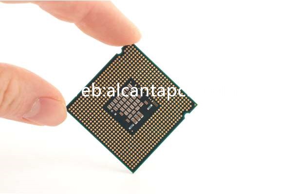
極薄IC (集積回路) パッケージ 基板 現代のエレクトロニクスにおいて重要なコンポーネントです, さまざまな機器の小型化・高性能化を可能にします. これらの基板は、必要な電気的特性を維持しながら、非常に薄く設計されています。, 熱, 高性能ICをサポートする機械的特性と. 超薄型基板は、スペースが貴重な用途において特に重要です, スマートフォンなどの, ウェアラブルデバイス, および高度なコンピューティング システム.
超薄型ICパッケージ基板とは?
超薄型ICパッケージ基板は、特殊なタイプのプリント基板です。 (プリント基板) ICの実装と相互接続のためのプラットフォームを提供するように設計されています. これらの基板の特徴は、最小限の厚さです。, 通常は以下です 100 マイクロメートル, これにより、超小型の電子パッケージの開発が可能になります。. 薄さにもかかわらず, 極薄基板は高密度の相互接続をサポートする必要がある, 効率的な熱管理, ホストする IC の信頼性の高い動作を保証する堅牢な機械的安定性.
超薄型 IC パッケージ基板設計リファレンス ガイド
超薄型 IC パッケージ基板の設計には、最適なパフォーマンスと信頼性を確保するための包括的なアプローチが必要です.
極薄基板で望ましい特性を達成するには、材料の選択が重要です:
高密度ポリイミドフィルム: これらの材料は優れた柔軟性を備えています, 高い熱安定性, 優れた電気絶縁性, 極薄アプリケーションに最適です.
銅箔: 導電性トレースおよび相互接続に使用されます, 銅箔は、かさばらずに電気的性能を維持するために、薄くても耐久性がなければなりません。.
接着剤と誘電体: 層を接着し、絶縁を提供するために、低誘電率と高熱伝導率を備えた高度な接着剤と誘電材料が使用されています。.
極薄基板の層構造は、スペース効率とパフォーマンスを最大化するように設計されています。:
シグナルレイヤー: これらの層は信号損失とクロストークを最小限に抑えるように構成されています. 制御されたインピーダンスを維持するために、マイクロストリップやストリップラインなどの技術が使用されます.
電源層とグランド層: 専用の電源プレーンとグランドプレーンは、安定した電力供給とノイズ低減に不可欠です, ICの信頼性の高い動作を保証する.
熱管理層: サーマルビアとヒートスプレッダを統合することで、熱を効果的に放散します。, 重要なコンポーネントの過熱を防止.
相互接続層: 高密度相互接続 (HDI) マイクロビアとスルーホールを使用すると、極薄基板の限られたスペース内で複雑な配線が可能になります.
超薄型ICパッケージ基板にはどのような材料が使用されているのか?
超薄型 IC パッケージ基板に使用される材料は、厳しい性能要件を満たすことができるように選択されています。:
高密度ポリイミドフィルム: 優れた柔軟性を提供, 熱安定性, 電気絶縁性, これらのフィルムは極薄用途によく選ばれます.
銅箔: 導電性トレースと相互接続には、薄くて耐久性のある銅箔が使用されています, 信頼性の高い電気的性能を保証する.
接着剤と誘電体: 層を接着し、絶縁を提供するために、低誘電率と高熱伝導率を備えた高度な接着剤と誘電材料が使用されています。.
強化エポキシ樹脂: これらの材料は、薄型を維持しながら基板の機械的強度を強化します。.
超薄型ICパッケージ基板のサイズはどのくらいですか?
超薄型 IC パッケージ基板のサイズは、特定のアプリケーションやデバイスの要件によって異なります。:
厚さ: 極薄基板は通常、 100 マイクロメートルの厚さ, 一部の設計では、最小のフォームファクタに対応するためにさらに薄い厚さに達しています。.
長さと幅: これらの寸法は、IC のサイズと相互接続のレイアウトによって決まります。. 一般的なサイズは、小型 IC の場合は数ミリメートル、大型パッケージの場合は数センチメートルに及びます。.
超薄型ICパッケージ基板の製造プロセス
超薄型 IC パッケージ基板の製造プロセスには、高品質とパフォーマンスを確保するために正確に制御されたいくつかのステップが含まれます:
高密度ポリイミドフィルム, 導電性材料, 接着剤が準備され、加工に適したサイズに切断されます。.
層は、導電性材料と絶縁性材料を積層して製造されます。. 各層はフォトリソグラフィーを使用してパターン化され、回路を定義します。.
マイクロビアとスルーホールは、レーザーまたは機械的穴あけ技術を使用して穴あけされます。. これらの穴は銅でめっきされ、層間に電気接続が形成されます。.
フォトリソグラフィーとエッチングプロセスを使用して、各層にファインピッチ回路を作成します. このステップでは、正確で信頼性の高い相互接続を確保するために高い精度が必要です。.
層作製後, 熱と圧力の下で層を貼り合わせます. 組み立てられた基板は厳格なテストを受けます, 電気試験を含む, 熱サイクル, および機械的ストレステスト, パフォーマンスと信頼性を確保するために.
超薄型ICパッケージ基板の応用分野
超薄型 IC パッケージ基板により、幅広いアプリケーションで高度な機能が可能になります:
スマートフォンで, 錠剤, およびウェアラブルデバイス, 超薄型基板は、高度な IC のコンパクトで効率的な統合をサポートします。, サイズと重量を削減しながら、パフォーマンスと機能を向上させます.
サーバー内, データセンター, そしてスーパーコンピューター, 超薄型基板により、強力なプロセッサとメモリ モジュールをコンパクトなフォーム ファクタに統合できます。, 高速なデータ処理と保存を容易にする.
これらの基板は通信インフラに不可欠です, 基地局やネットワーク機器を含む, コンパクトな設置面積で信頼性の高い高速接続を提供します.
さまざまな家電製品に, スマートホームデバイスからゲームコンソールまで, 極薄基板により、洗練されたデザインで高性能を実現, スペース効率の高い設計.
医療画像および診断装置において, 超薄型基板が高速データ取得と処理をサポート, 医療処置の精度と効率の向上.
超薄型ICパッケージ基板のメリットとは?
超薄型 IC パッケージ基板には、高度な電子アプリケーションに不可欠ないくつかの利点があります。:
コンパクトデザイン: 超薄型プロファイルにより、電子パッケージの小型化が可能になります。, よりコンパクトでポータブルなデバイスを実現.
高性能: 最適化された材料と設計により、高い信号整合性が保証されます, 低電力損失, 効果的な熱管理.
信頼性の向上: 高度な製造プロセスと材料により高い信頼性を実現, 要求の厳しい環境でも長期的なパフォーマンスを確保.
柔軟性: これらの基板は薄くて柔軟性があるため、幅広い用途に適しています。, 堅固な高性能デバイスから柔軟でウェアラブルなエレクトロニクスまで.
スケーラビリティ: 極薄基板は、さまざまな用途の特定のニーズを満たすようにカスタマイズできます。, 小型の民生用デバイスから大規模な産業用システムまで.
よくある質問
超薄型 IC パッケージ基板を設計する際の重要な考慮事項は何ですか??
主な考慮事項には、電気特性と熱特性を考慮した材料の選択が含まれます, シグナルインテグリティと熱管理のための層構造の最適化, 機械的な安定性と信頼性を確保する.
超薄型 IC パッケージ基板は標準 PCB とどう違うのか?
超薄型 IC パッケージ基板が大幅に薄くなりました, より多くの層とより高い相互接続密度, 標準の PCB と比較して、より高い周波数と電力レベルを処理できるように設計されています, 高度なアプリケーションに適したものにする.
超薄型 IC パッケージ基板の一般的な製造プロセスは何ですか??
プロセスには材料の準備が含まれます, 層の製造, 穴あけとメッキ, 回路パターニング, 組み立て, 高いパフォーマンスと信頼性を保証するための厳格なテスト.
超薄型 IC パッケージ基板の主な用途は何ですか??
これらの基板はモバイル機器に使用されています, ハイパフォーマンスコンピューティング, 電気通信, 家電, および医療機器, これらの分野で高度な機能と信頼性を提供します.