المحدودة")
الشركة المصنعة لمركبات ثنائي الفينيل متعدد الكلور لتجويف الهوائي, نحن متخصصون في إنشاء لوحات دوائر مطبوعة عالية الأداء مصممة لتطبيقات الهوائيات المتقدمة. تكمن خبرتنا في الهندسة الدقيقة وعمليات التصنيع المتطورة, ضمان سلامة الإشارة الأمثل والحد الأدنى من التدخل. نحن نقدم حلولاً مخصصة مصممة خصيصًا لتلبية الاحتياجات الملحة لصناعات مثل الاتصالات, الفضاء الجوي, والدفاع. مع الالتزام بالجودة والابتكار, نحن نقدم موثوقة, هوائي عالي التردد تجويف مركبات ثنائي الفينيل متعدد الكلور التي تدفع الاتصال والأداء الفائق في الأنظمة الحيوية.
تجويف الهوائي ثنائي الفينيل متعدد الكلور (لوحات الدوائر المطبوعة) هي لوحات دوائر متخصصة مصممة لدمج الهوائيات داخل هيكل التجويف, تحسين أداء الترددات اللاسلكية (تردد الراديو) وتطبيقات الميكروويف. تعد مركبات ثنائي الفينيل متعدد الكلور هذه ضرورية في التطبيقات التي تتطلب إرسال إشارات عالية التردد, مثل الاتصالات السلكية واللاسلكية, الفضاء الجوي, وأنظمة الدفاع. تستكشف هذه المقالة الخصائص, اعتبارات التصميم, مواد, عمليات التصنيع, التطبيقات, ومزايا تجويف الهوائي مركبات ثنائي الفينيل متعدد الكلور.
ما هي ثنائي الفينيل متعدد الكلور تجويف الهوائي?
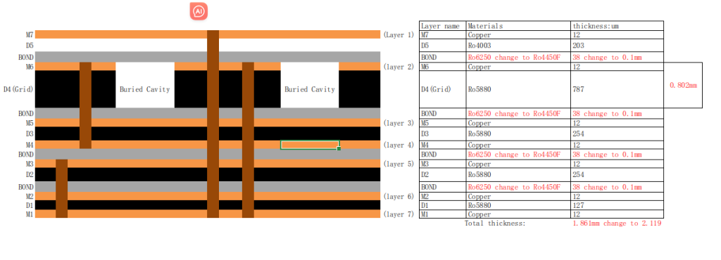
تشتمل مركبات ثنائي الفينيل متعدد الكلور الموجودة في تجويف الهوائي على تجاويف داخل هيكل ثنائي الفينيل متعدد الكلور لإيواء الهوائيات, توفير بيئة خاضعة للرقابة تعزز أداء الإشارة. تم تصميم هذه التجاويف لتحسين الخصائص الكهرومغناطيسية, تقليل فقدان الإشارة, وتحسين الكفاءة الشاملة للهوائي. يتيح دمج الهوائيات داخل هيكل ثنائي الفينيل متعدد الكلور تصميمات مدمجة وفعالة, مما يجعلها مناسبة للتطبيقات عالية التردد.
اعتبارات التصميم لثنائي الفينيل متعدد الكلور تجويف الهوائي
تصميم تجويف الهوائي ثنائي الفينيل متعدد الكلور ينطوي على عدة اعتبارات حاسمة:
الشكل, مقاس, يعد وضع التجويف أمرًا ضروريًا لتحسين الخصائص الكهرومغناطيسية وأداء الهوائي.
اختيار مواد PCB المناسبة التي توفر فقدًا منخفضًا للعزل الكهربائي, الموصلية الحرارية العالية, والأداء المستقر عبر الترددات أمر ضروري.
يعد ضمان مطابقة المعاوقة المناسبة بين الهوائي وبقية الدوائر أمرًا حيويًا لتقليل انعكاس الإشارة وفقدانها.
يجب تنفيذ تقنيات الإدارة الحرارية الفعالة لتبديد الحرارة الناتجة عن الإشارات عالية التردد.
تقنيات التدريع المناسبة ضرورية لمنع التداخل الكهرومغناطيسي (إيمي) وضمان نقل الإشارات النظيفة.
يعد الحفاظ على تفاوتات التصنيع الصارمة أمرًا بالغ الأهمية لضمان الأداء والموثوقية المتسقة.
المواد المستخدمة في ثنائي الفينيل متعدد الكلور تجويف الهوائي
يتم استخدام العديد من المواد بشكل شائع في تصنيع مركبات ثنائي الفينيل متعدد الكلور لتجويف الهوائي:
مواد مثل Rogers RT/duroid, 4000 ريال عماني, وسلسلة RO3000 توفر خسارة عازلة منخفضة وأداء مستقر عبر الترددات العالية.
توفر هذه المواد خصائص حرارية وكهربائية ممتازة, مما يجعلها مناسبة للتطبيقات عالية التردد.
يستخدم النحاس في الآثار الموصلة وجدران التجاويف بسبب موصليته الكهربائية الممتازة.
تيمز, مثل الشحوم الحرارية أو الفوط, تستخدم لتعزيز انتقال الحرارة بين المكونات وحلول التبريد.
المواد الموصلة, مثل النحاس أو الألومنيوم, تستخدم للتدريع لمنع EMI.
عملية تصنيع مركبات ثنائي الفينيل متعدد الكلور ذات تجويف الهوائي
تتضمن عملية تصنيع مركبات ثنائي الفينيل متعدد الكلور ذات تجويف الهوائي عدة خطوات دقيقة:
يتم تحضير شرائح عالية التردد ومواد أخرى ومعالجتها إلى صفائح أو أفلام.
يتم إنشاء التجاويف داخل طبقات ثنائي الفينيل متعدد الكلور باستخدام تقنيات التصنيع أو الحفر الدقيقة.
طبقات ثنائي الفينيل متعدد الكلور, بما في ذلك التجويف, مكدسة وفقا للتصميم, مع دراسة متأنية لوضع المواد العازلة والآثار الموصلة.
يتم حفر المنافذ وطلائها لإنشاء وصلات كهربائية عمودية بين الطبقات المختلفة والتجويف.
عناصر, بما في ذلك الهوائي, يتم تركيبها على PCB باستخدام تقنية التركيب الآلي على السطح (سمت) العمليات.
بالوعة الحرارة, مراوح التبريد, ويتم دمج مواد الواجهة الحرارية لضمان الإدارة الحرارية الفعالة.
يتم تطبيق مواد التدريع لمنع EMI وضمان نقل الإشارات النظيفة.
تخضع اللوحات المجمعة لاختبارات وفحص صارم للتأكد من أنها تلبي المواصفات المطلوبة للأداء الكهربائي, سلامة الإشارة, والموثوقية.
يتم تجميع اللوحات التي تم اختبارها والتحقق من صحتها في شكلها النهائي, معبأة, وجاهزة للتوزيع.
تطبيقات ثنائي الفينيل متعدد الكلور تجويف الهوائي
تُستخدم مركبات ثنائي الفينيل متعدد الكلور الموجودة في تجويف الهوائي في مجموعة واسعة من التطبيقات عالية التردد:
يتم استخدام مركبات ثنائي الفينيل متعدد الكلور هذه في المحطات الأساسية, هوائيات, وأجهزة الاتصال الأخرى حيث يعد إرسال الإشارات عالية التردد أمرًا بالغ الأهمية.
تعد مركبات ثنائي الفينيل متعدد الكلور الموجودة في تجويف الهوائي ضرورية في أنظمة الرادار, الاتصالات عبر الأقمار الصناعية, والإلكترونيات العسكرية, حيث الموثوقية والأداء أمر بالغ الأهمية.
تُستخدم مركبات ثنائي الفينيل متعدد الكلور هذه في معدات التصوير الطبي والتشخيص التي تعمل بترددات عالية, تتطلب نقل إشارة دقيق وموثوق.
تُستخدم مركبات ثنائي الفينيل متعدد الكلور الموجودة في تجويف الهوائي في أنظمة مساعدة السائق المتقدمة (ADAS), مركبة إلى كل شيء (V2X) تواصل, وأنظمة الرادار.
وتستخدم مركبات ثنائي الفينيل متعدد الكلور هذه في أجهزة الاستشعار الصناعية, أنظمة الأتمتة, وغيرها من التطبيقات الصناعية عالية التردد.
مزايا ثنائي الفينيل متعدد الكلور تجويف الهوائي
تقدم مركبات ثنائي الفينيل متعدد الكلور الموجودة في تجويف الهوائي العديد من المزايا:
يقلل هيكل التجويف من فقدان الإشارة والتداخل, تحسين قوة الإشارة ووضوحها.
يتيح دمج الهوائيات داخل PCB تصميمات أكثر إحكاما, توفير المساحة وتقليل الحجم الكلي للجهاز.
تعمل بيئة التجويف الخاضعة للرقابة على حماية الهوائي من العوامل البيئية, تعزيز الموثوقية وطول العمر.
تم تصميم مركبات ثنائي الفينيل متعدد الكلور هذه لتعمل بكفاءة عند الترددات العالية, مما يجعلها مناسبة لتطبيقات الترددات اللاسلكية والميكروويف.
يمكن تصميم مركبات ثنائي الفينيل متعدد الكلور في تجويف الهوائي وفقًا لمتطلبات محددة, بما في ذلك نطاق التردد, التعامل مع السلطة, والظروف البيئية.
التعليمات
ما هي الفوائد الرئيسية لاستخدام ثنائي الفينيل متعدد الكلور تجويف الهوائي?
وتشمل الفوائد الرئيسية تعزيز أداء الإشارة, تصميم مدمج, تحسين الموثوقية, قدرة عالية التردد, والتخصيص. هذه المزايا تجعل مركبات ثنائي الفينيل متعدد الكلور الموجودة في تجويف الهوائي مثالية للتطبيقات عالية التردد وعالية الطاقة.
ما هي المواد المستخدمة عادة في ثنائي الفينيل متعدد الكلور تجويف الهوائي?
تشمل المواد الشائعة شرائح عالية التردد مثل Rogers RT/duroid, 4000 ريال عماني, وسلسلة RO3000, PTFE مملوء بالسيراميك, النحاس للآثار الموصلة وجدران التجاويف, مواد الواجهة الحرارية (تيمز), ومواد التدريع مثل النحاس أو الألومنيوم.
كيف يضمن تصميم تجويف الهوائي PCB الأداء العالي?
يضمن التصميم الأداء العالي من خلال تحسين تصميم التجويف, اختيار المواد المناسبة, ضمان مطابقة المعاوقة المناسبة, تنفيذ الإدارة الحرارية الفعالة, تطبيق تقنيات التدريع المناسبة, والحفاظ على التحمل التصنيعي الصارم.
ما هي التطبيقات الشائعة لثنائي الفينيل متعدد الكلور تجويف الهوائي?
وتشمل التطبيقات الشائعة الاتصالات السلكية واللاسلكية (محطات القاعدة, هوائيات), الفضاء والدفاع (أنظمة الرادار, الاتصالات عبر الأقمار الصناعية), الأجهزة الطبية (التصوير الطبي, التشخيص), إلكترونيات السيارات (ADAS, الاتصالات V2X), والتطبيقات الصناعية (أجهزة استشعار, أنظمة الأتمتة). تُستخدم مركبات ثنائي الفينيل متعدد الكلور هذه في الأنظمة التي تتطلب أداءً عالي التردد ونقلًا موثوقًا للإشارات.