المحدودة")
الشركة المصنعة لـ Cavity-PCB. تتطلب مركبات PCB ذات التجويف المفتوح فتحة يتم التحكم فيها بعمق لتعريض الطبقات الداخلية للهواء لتجميع الهوائي أو المكونات. ينتج مصنع Alcanta PCB العديد من أنواع لوحات تجويف PCB. تجاويف على لوحات ثنائي الفينيل متعدد الكلور. معظم التصميم. عليك أن تضع بعض IC الرئيسي (أجزاء) في التجاويف. نعم. يمكننا إنتاج هذه الأنواع لوحات تجويف بجودة عالية. يمكننا أن نجعل تجويف ثنائي الفينيل متعدد الكلور من 4 طبقة ل 70 طبقات. معظم التجويف من 4 طبقة ل 16 طبقات.
في بعض المجالات الخاصة. سوف تستخدم تجاويف ثنائي الفينيل متعدد الكلور مواد ثنائي الفينيل متعدد الكلور عالي السرعة, مواد ثنائي الفينيل متعدد الكلور عالية التردد, المواد المعدنية, مواد عالية TG FR4, أو غيرها من مواد ثنائي الفينيل متعدد الكلور المختلفة. يمكننا إنتاج جميع هذه الأنواع من ألواح تجاويف المواد. جودة عالية, وأكثر أرخص الأسعار. عند تصميم هذا النوع من تجاويف ثنائي الفينيل متعدد الكلور. إذا كان لديك بعض الأسئلة. يمكنك التحقق معنا. سنساعدك في أي وقت. لا تحتاج إلى أي دفع. مجرد تبادل فني.

ال تجاويف تقنيات ثنائي الفينيل متعدد الكلور. نعم. يمكننا صنع ألواح التجويف بالعديد من التقنيات المتقدمة. عينة: يمكننا أن نجعل تجويف ثنائي الفينيل متعدد الكلور مع Vias مدفونة ومكفوفة. يرجى الانتباه إلى معرفة. في منطقة التجاويف. هناك بعض الثقوب المدفونة أو المسدودة. أعني. سوف تظهر الثقوب عبر جانب النحاس في منطقة التجويف.
حول المواد العازلة. إذا كنت في حاجة. يمكننا أن نجعل تجاويف ثنائي الفينيل متعدد الكلور مع العديد من المواد العازلة المختلفة. يحب: روجرز العوازل العوازل VS FR4, أو, عوازل روجرز VS عوازل إيزولا, أو م7, م4, عوازل M6, وغيرها أداء عالي, عوازل FR4 منخفضة الخسارة. فقط أخبرنا. ما هي أنواع العوازل الكهربائية التي تحتاجها؟? أخبرنا من فضلك. يمكننا إنتاجه. والقيام بعمل جيد.
حول تكنولوجيا إنتاج تجويف ثنائي الفينيل متعدد الكلور الأخرى. يحب: التحكم في المعاوقة. يمكننا أن نفعل +/-5%, الحفر الخلفي, التحكم في العمق والحفر, جامدة-فليكس & الدوائر المرنة, وغيرها. أنتجت شركتنا العديد من منتجات ثنائي الفينيل متعدد الكلور العسكرية, الطيران ثنائي الفينيل متعدد الكلور, الاتصالات العسكرية ثنائي الفينيل متعدد الكلور, منتج ثنائي الفينيل متعدد الكلور الصناعي, والعديد من المنتجات في المجالات الأخرى.
مزيد من المعلومات حول تجويف ثنائي الفينيل متعدد الكلور: ما هو تجويف ثنائي الفينيل متعدد الكلور?
في عالم الإلكترونيات الديناميكي, الابتكار ثابت, مما أدى إلى ظهور تقنيات متخصصة مثل تجويف ثنائي الفينيل متعدد الكلور. توفر لوحات الدوائر الفريدة هذه مزايا مميزة في تطبيقات محددة, ثورة في الصناعات حيث الدقة والأداء لها أهمية قصوى. تتعمق هذه المقالة في مفهوم تجويف ثنائي الفينيل متعدد الكلور, تسليط الضوء على بنائها, التطبيقات, والفوائد.
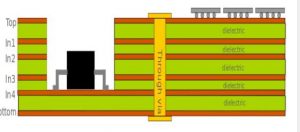
فهم تجويف ثنائي الفينيل متعدد الكلور: تجويف مركبات ثنائي الفينيل متعدد الكلور, تُعرف أيضًا باسم ألواح ثنائي الفينيل متعدد الكلور المدعومة بالتجويف أو ألواح التجويف, هي نوع متخصص من لوحات الدوائر المطبوعة التي تحتوي على منطقة غائرة واحدة أو أكثر, أو تجاويف, تشكيله في واحد أو كلا الجانبين. يمكن أن تختلف هذه المناطق المريحة في الشكل, عمق, والحجم, اعتمادا على متطلبات التطبيق.
بناء تجويف ثنائي الفينيل متعدد الكلور: يتضمن بناء تجاويف ثنائي الفينيل متعدد الكلور عمليات تصنيع ثنائي الفينيل متعدد الكلور التقليدية مع خطوة إضافية - طحن أو توجيه التجاويف على سطح اللوحة(ق). CNC المتقدم (التحكم العددي بالكمبيوتر) تقوم معدات التصنيع أو التوجيه بنحت هذه التجاويف بدقة, تاركين وراءهم الركيزة التي تشكل قاعدة التجويف أو جدرانه. تضمن هذه العملية الدقيقة السلامة الهيكلية مع تلبية متطلبات التصميم المتخصصة لثنائي الفينيل متعدد الكلور.
تطبيقات تجويف ثنائي الفينيل متعدد الكلور: تجد مركبات ثنائي الفينيل متعدد الكلور المجوفة استخدامًا واسع النطاق في مختلف الصناعات حيث الأداء, مصداقية, وسلامة الإشارة أمر بالغ الأهمية. وتشمل بعض التطبيقات البارزة:
- أنظمة الترددات اللاسلكية والميكروويف: تتفوق مركبات ثنائي الفينيل متعدد الكلور المجوفة في تطبيقات الترددات اللاسلكية والميكروويف, وخاصة في أنظمة الهوائي ومعدات الاتصالات. يعمل التجويف كدرع, تقليل التداخل الكهرومغناطيسي وتعزيز إرسال الإشارات واستقبالها.
- إلكترونيات عالية التردد: في الدوائر عالية التردد مثل أنظمة الرادار, الأجهزة اللاسلكية, والاتصالات الأقمار الصناعية, توفر مركبات ثنائي الفينيل متعدد الكلور المجوفة أداءً فائقًا من خلال تقليل فقدان الإشارة والضوضاء, وبالتالي تحسين كفاءة النظام بشكل عام.
- الفضاء والدفاع: يستفيد قطاعا الطيران والدفاع من مركبات ثنائي الفينيل متعدد الكلور المجوفة في أنظمة المهام الحرجة مثل إلكترونيات الطيران, مصفوفات الرادار, وأنظمة توجيه الصواريخ. إن تصميمها القوي وسلامة الإشارة الاستثنائية يجعلها لا غنى عنها في هذه البيئات الصعبة.
- الالكترونيات الطبية: في الأجهزة الطبية ومعدات التشخيص, تلعب مركبات ثنائي الفينيل متعدد الكلور المجوفة دورًا حيويًا في ضمان قراءات وتشخيصات دقيقة. إن قدرتها على تقليل التداخل والحفاظ على وضوح الإشارة لا تقدر بثمن في التطبيقات الطبية الحساسة.
فوائد تجويف ثنائي الفينيل متعدد الكلور: تقدم مركبات ثنائي الفينيل متعدد الكلور المجوفة العديد من الفوائد الرئيسية, مشتمل:
- تعزيز سلامة الإشارة: تصميم التجويف يقلل من التداخل الكهرومغناطيسي, مما يؤدي إلى نقل إشارة أنظف وتحسين الأداء العام, وخاصة في التطبيقات عالية التردد.
- تحسين الإدارة الحرارية: تعمل مركبات ثنائي الفينيل متعدد الكلور المجوفة على تسهيل تبديد الحرارة بشكل أفضل, حاسم للمكونات الإلكترونية التي تعمل في البيئات الحرارية الصعبة, وبالتالي تعزيز موثوقية النظام وطول العمر.
- تحسين المساحة: من خلال دمج المكونات داخل التجويف, تتيح مركبات ثنائي الفينيل متعدد الكلور المجوفة تصميمات مدمجة وخفيفة الوزن, مما يجعلها مثالية للتطبيقات ذات المساحة المحدودة حيث يكون الحجم والوزن من العوامل الحاسمة.
خاتمة: تمثل مركبات ثنائي الفينيل متعدد الكلور المجوفة حلاً متخصصًا مصممًا خصيصًا لتلبية المتطلبات الفريدة للأنظمة الإلكترونية الحديثة. مع تصميمها المتقدم, البناء الدقيق, وخصائص الأداء المتفوق, تستمر مركبات ثنائي الفينيل متعدد الكلور المجوفة في دفع الابتكار عبر مجموعة واسعة من الصناعات, دفع حدود ما هو ممكن في التصميم والتصنيع الإلكتروني.
كيفية تصميم ثنائي الفينيل متعدد الكلور?
تصميم ثنائي الفينيل متعدد الكلور: دليل شامل:
تصميم لوحة الدوائر المطبوعة (ثنائي الفينيل متعدد الكلور) هي مهارة أساسية لعشاق الإلكترونيات والمهنيين على حد سواء. سواء كنت تقوم بإنشاء مشروع هواية بسيط أو جهاز إلكتروني معقد, فهم عملية تصميم ثنائي الفينيل متعدد الكلور أمر ضروري. توفر هذه المقالة دليلاً موجزًا وشاملاً لتصميم ثنائي الفينيل متعدد الكلور, تغطي الخطوات والاعتبارات الرئيسية على طول الطريق.
خطوة 1: تحديد المتطلبات ابدأ بتحديد متطلبات ثنائي الفينيل متعدد الكلور بوضوح. النظر في عوامل مثل الحجم, الوظيفة, متطلبات الطاقة, والظروف البيئية التي ستعمل فيها. إن فهم هذه المتطلبات مقدمًا سيوجه عملية التصميم بأكملها.
خطوة 2: التصميم التخطيطي قم بإنشاء رسم تخطيطي لدائرتك باستخدام أتمتة التصميم الإلكتروني (جمعية الإمارات للغوص) برمجة. يعمل هذا المخطط كمخطط للاتصالات بين المكونات ويحدد السلوك الكهربائي للدائرة. ضمان الدقة والاكتمال في مرحلة التصميم التخطيطي.
خطوة 3: اختيار المكونات وموضعها حدد المكونات بناءً على وظائفها, التوفر, والتكلفة. بمجرد اختياره, ضع المكونات على تخطيط ثنائي الفينيل متعدد الكلور وفقًا للرسم التخطيطي. النظر في عوامل مثل توجيه الإشارة, الإدارة الحرارية, وسهولة التجميع أثناء وضع المكونات.
خطوة 4: تخطيط ثنائي الفينيل متعدد الكلور انتقل إلى مرحلة تخطيط ثنائي الفينيل متعدد الكلور بعد وضع المكونات. قم بترتيب المكونات الموجودة على PCB لتحسين سلامة الإشارة, تقليل التدخل, وضمان التوجيه الفعال. انتبه إلى عوامل مثل طول التتبع, التحكم في المعاوقة, ومسارات عودة الإشارة أثناء تصميم التخطيط.
خطوة 5: التوجيه قم بتوصيل المكونات الموجودة على تخطيط PCB عن طريق توجيه الآثار فيما بينها. اتبع أفضل الممارسات لتوجيه التتبع, مثل الحفاظ على عروض تتبع متسقة, تجنب الزوايا الحادة, والتقليل من الحديث المتبادل للإشارة. استخدم الطائرات الأرضية والطاقة لتوفير توزيع مستقر للجهد وتقليل التداخل الكهرومغناطيسي.
خطوة 6: التحقق من قواعد التصميم (جمهورية الكونغو الديمقراطية) قم بإجراء فحص لقواعد التصميم للتأكد من أن تصميم ثنائي الفينيل متعدد الكلور الخاص بك يتوافق مع قيود التصنيع ومعايير الصناعة. التحقق من وجود مخالفات التخليص, الحد الأدنى من عروض التتبع, وأحجام الوسادة الصحيحة. قم بمعالجة أي أخطاء أو تحذيرات تم تحديدها أثناء عملية DRC.
خطوة 7: التحقق من التصميم قبل التصنيع, التحقق من وظائف وسلامة تصميم PCB الخاص بك من خلال المحاكاة والاختبار. استخدم برامج المحاكاة للتحقق من صحة الأداء مقابل مواصفات التصميم. قم بإنشاء نموذج أولي واختبار لثنائي الفينيل متعدد الكلور لتحديد أي مشكلات وإجراء التعديلات اللازمة.
خطوة 8: إنشاء ملفات التصنيع بمجرد الانتهاء والتحقق منها, إنشاء ملفات التصنيع اللازمة للتصنيع. تتضمن هذه الملفات عادةً ملفات Gerber للأعمال الفنية لثنائي الفينيل متعدد الكلور, ملفات الحفر لوضع الثقب, وفاتورة المواد (بوم) تفاصيل مواصفات المكونات. قم بمراجعة ملفات التصنيع للتأكد من دقتها قبل إرسالها إلى الشركة المصنعة لثنائي الفينيل متعدد الكلور.
خطوة 9: التصنيع والتجميع قم بإرسال ملفات التصنيع إلى منشأة تصنيع ثنائي الفينيل متعدد الكلور للإنتاج. اختر شركة مصنعة ذات سمعة طيبة تقدم خدمات تصنيع عالية الجودة. عند استلام مركبات ثنائي الفينيل متعدد الكلور ملفقة, تابع تجميع المكونات واللحام وفقًا لقائمة مكونات الصنف وتعليمات التجميع.
خاتمة: يتطلب تصميم ثنائي الفينيل متعدد الكلور تخطيطًا دقيقًا, الاهتمام بالتفاصيل, والالتزام بأفضل الممارسات. باتباع هذا الدليل, يمكنك إنشاء ثنائي الفينيل متعدد الكلور مصمم جيدًا والذي يلبي متطلبات مشروعك ويعمل بشكل موثوق في التطبيق المقصود. حسّن مهاراتك في التصميم باستمرار وابق على اطلاع دائم بالتطورات في تكنولوجيا ثنائي الفينيل متعدد الكلور لمواجهة تحديات التصميم المتزايدة التعقيد بثقة.
كيفية تصنيع تجويف ثنائي الفينيل متعدد الكلور?
عملية تصنيع تجويف ثنائي الفينيل متعدد الكلور: دليل شامل:
تجويف مركبات ثنائي الفينيل متعدد الكلور, المعروف أيضًا باسم مركبات ثنائي الفينيل متعدد الكلور المدعومة بالتجويف, تمثل نوعًا متخصصًا من لوحات الدوائر المطبوعة ذات مناطق غائرة أو تجاويف يتم تشكيلها في أحد الجانبين أو كليهما. تتضمن عملية تصنيع مركبات ثنائي الفينيل متعدد الكلور المجوفة خطوات فريدة لتحقيق الدقة والموثوقية. توفر هذه المقالة نظرة عامة على عملية التصنيع, تسليط الضوء على الخطوات والاعتبارات الرئيسية.
خطوة 1: التصميم والمواصفات تبدأ عملية تصنيع مركبات ثنائي الفينيل متعدد الكلور المجوفة بمرحلة التصميم, حيث يحدد المهندسون التخطيط, أبعاد, ومواصفات البورد. وهذا يشمل تحديد الموقع, مقاس, وعمق التجاويف, وكذلك اختيار المواد والتشطيبات التي تلبي متطلبات التطبيق.
خطوة 2: اختيار المواد يعد اختيار مادة الركيزة المناسبة أمرًا بالغ الأهمية لتجويف مركبات ثنائي الفينيل متعدد الكلور. تشمل المواد الشائعة FR-4, روجرز, وعالية التردد شرائح, تم اختياره بناءً على عوامل مثل ثابت العزل الكهربائي, الموصلية الحرارية, والقوة الميكانيكية. توفر المادة الأساسية الأساس لثنائي الفينيل متعدد الكلور وتؤثر على خصائصه الكهربائية والميكانيكية.
خطوة 3: التصنيع باستخدام الحاسب الآلي بمجرد الانتهاء من التصميم واختيار المواد, تنتقل عملية التصنيع إلى CNC (التحكم العددي بالكمبيوتر) بالقطع. استخدام معدات الطحن أو التوجيه الدقيقة, يقوم الفنيون بنحت التجاويف الموجودة على ركيزة ثنائي الفينيل متعدد الكلور بعناية وفقًا لمواصفات التصميم. تضمن المعالجة باستخدام الحاسب الآلي الدقة والاتساق في أبعاد التجويف وموضعه.
خطوة 4: تكديس الطبقات وتصفيحها بعد معالجة التجاويف, والخطوة التالية هي تكديس الطبقة والتصفيح. يتم وضع طبقات متعددة من رقائق النحاس والتجهيز المسبق بين طبقات الركيزة لتشكيل مجموعة PCB. يتم بعد ذلك ضغط هذا المكدس معًا تحت درجة حرارة وضغط مرتفعين باستخدام عملية التصفيح, ربط الطبقات في طبقة واحدة, هيكل متماسك.
خطوة 5: الحفر والطلاء بمجرد تصفيح مجموعة ثنائي الفينيل متعدد الكلور, يتم استخدام معدات الحفر الدقيقة لإنشاء ثقوب لتركيب المكونات والتوصيلات الكهربائية. بعد الحفر, الثقوب مطلية بالنحاس لتأسيس التوصيل الكهربائي وضمان الترابط الموثوق بين الطبقات.
خطوة 6: نقش ونقش الدوائر تتضمن المرحلة التالية نقش آثار الدائرة وميزاتها على طبقات ثنائي الفينيل متعدد الكلور. يتم تطبيق مادة مقاومة للضوء على الأسطح النحاسية, يليه التعرض للأشعة فوق البنفسجية من خلال قناع ضوئي, الذي يحدد نمط الدائرة المطلوب. ثم يتم حفر المناطق المكشوفة باستخدام المحاليل الكيميائية, تاركاً وراءه آثار وملامح النحاس المطلوبة.
خطوة 7: الانتهاء من السطح والتجمع بعد النقش, يخضع PCB لعمليات تشطيب السطح لحماية آثار النحاس وتعزيز قابلية اللحام. تشمل التشطيبات السطحية الشائعة HASL (التسوية لحام الهواء الساخن), يوافق (انغماس النيكل المنحل بالكهرباء), و OSP (المواد الحافظة العضوية القابلة للحام). أخيراً, يتم تجميع المكونات على PCB باستخدام آلات الالتقاط والمكان الآلية, ويتم لحامها في مكانها باستخدام تقنيات اللحام بإعادة التدفق أو اللحام الموجي.
خاتمة: تتطلب عملية تصنيع مركبات ثنائي الفينيل متعدد الكلور المجوفة الدقة, خبرة, والاهتمام بالتفاصيل في كل خطوة. من التصميم واختيار المواد إلى التصنيع باستخدام الحاسب الآلي, التصفيح, والتجمع, تلعب كل مرحلة دورًا حاسمًا في إنتاج مركبات ثنائي الفينيل متعدد الكلور عالية الجودة والتي تلبي المتطلبات الصارمة للتطبيقات الإلكترونية الحديثة. من خلال اتباع أفضل الممارسات والاستفادة من تقنيات التصنيع المتقدمة, يمكن للمصنعين ضمان موثوقية وأداء مركبات ثنائي الفينيل متعدد الكلور المجوفة في مختلف الصناعات.
يمكننا إنتاج العديد من أنواع التجاويف في ألواح ثنائي الفينيل متعدد الكلور ذات الطبقة العالية. إذا كان لديك أي أسئلة, فلا تتردد في الاتصال بنا info@alcantapcb.com , سنكون سعداء بمساعدتك.