المحدودة")
Flip Chip Ball Grid Array الشركة المصنعة للركيزة. كشركة رائدة الوجه رقاقة الشركة المصنعة لركيزة مصفوفة الشبكة الكروية, نحن متخصصون في إنتاج ركائز عالية الأداء للتطبيقات الإلكترونية المتقدمة. تضمن عمليات التصنيع الحديثة لدينا الجودة والموثوقية الفائقة, تلبية متطلبات الصناعات مثل الاتصالات, الحوسبة, والسيارات. من خلال الاستفادة من التكنولوجيا المتطورة والتصميم المبتكر, نحن نقدم الحلول التي تعزز أداء الجهاز, دعم التصغير, وضمان السلامة الحرارية والإشارة القوية.
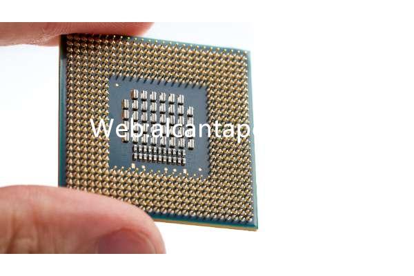
مصفوفة شبكة كرة Flip Chip (FC-BGA) الركيزة يعد عنصرًا حاسمًا في التغليف الإلكتروني الحديث, تقديم حل قوي للتطبيقات عالية الأداء وعالية الكثافة. تم تصميم ركائز FC-BGA لدعم رقائق أشباه الموصلات المتقدمة, توفير التوصيلات الكهربائية, الدعم الميكانيكي, وتبديد الحرارة. تلعب هذه الركائز دورًا محوريًا في تعزيز أداء وموثوقية الدوائر المتكاملة (المرحلية) في مختلف التطبيقات, تتراوح من الإلكترونيات الاستهلاكية إلى أنظمة السيارات. في هذه المقالة, سوف نتعمق في تعقيدات ركائز FC-BGA, استكشاف هيكلها, مواد, عمليات التصنيع, مجالات التطبيق, والمزايا.
ما هي الركيزة FC-BGA?
الركيزة FC-BGA هي نوع من تكنولوجيا التغليف المستخدمة لتركيب رقائق أشباه الموصلات مباشرة على الركيزة باستخدام نتوءات اللحام. على عكس ربط الأسلاك التقليدية, تعمل تقنية Flip Chip على قلب الشريحة رأسًا على عقب, السماح للمنطقة النشطة بمواجهة الركيزة. توفر هذه الطريقة العديد من المزايا, بما في ذلك التوصيلات البينية ذات الكثافة العالية, تحسين الأداء الكهربائي, وإدارة حرارية أفضل.
تتكون الركيزة FC-BGA من طبقات متعددة, بما في ذلك الطبقة الأساسية, طبقات البناء, وطبقات قناع اللحام. تتكون الطبقة الأساسية عادةً من مواد مثل البيسمالميد-تريازين (بي تي) الراتنج أو الايبوكسي, والتي توفر استقرارًا حراريًا ممتازًا وقوة ميكانيكية. طبقات البناء, مصنوعة من مواد عازلة والنحاس, تتم إضافتها لإنشاء الأسلاك المعقدة المطلوبة للتوصيلات البينية عالية الكثافة. تعمل طبقات قناع اللحام على حماية الدوائر وتمنع سد اللحام أثناء التجميع.
يتم تشكيل الترابط بين الشريحة والركيزة باستخدام نتوءات اللحام, وهي عبارة عن كرات صغيرة من مادة اللحام موضوعة على منصات الإدخال / الإخراج الخاصة بالرقاقة. أثناء التجميع, يتم قلب الشريحة ومحاذاتها مع الركيزة, ويتم إعادة تدفق نتوءات اللحام لإنشاء اتصال ميكانيكي وكهربائي قوي. تتيح هذه العملية عددًا أكبر من التوصيلات البينية لكل وحدة مساحة مقارنةً بربط الأسلاك التقليدية.
هيكل ركائز FC-BGA
هيكل ركائز FC-BGA معقد ومصمم هندسيًا للغاية لتلبية متطلبات تعبئة أشباه الموصلات المتقدمة. تتكون الركائز عادة من عدة مكونات رئيسية:
توفر الطبقة الأساسية العمود الفقري الميكانيكي للركيزة. تُستخدم مواد مثل راتنجات BT أو الإيبوكسي بشكل شائع نظرًا لخصائصها الحرارية والميكانيكية الممتازة. الطبقة الأساسية عادة ما تكون صلبة, توفير الاستقرار والدعم لهيكل الركيزة بأكمله.
تتم إضافة طبقات بناء متعددة على جانبي الطبقة الأساسية لإنشاء التوجيه اللازم للإشارات الكهربائية. هذه الطبقات مصنوعة من مواد عازلة, مثل النحاس المطلي بالراتنج (RCC) أو الايبوكسي, وتتخللها آثار نحاسية. تعمل الطبقات المتراكمة على تمكين الأسلاك عالية الكثافة المطلوبة للدوائر المرحلية المتقدمة, السماح بالتوجيه المعقد وطبقات متعددة من الترابط.
يتم تطبيق طبقات قناع اللحام أعلى الطبقات المتراكمة لحماية الدوائر ومنع سد اللحام. هذه الطبقات مصنوعة من مواد عازلة وهي ضرورية للحفاظ على سلامة التوصيلات الكهربائية أثناء التجميع والتشغيل.
نتوءات اللحام عبارة عن كرات صغيرة من مادة اللحام موضوعة على منصات الإدخال / الإخراج الخاصة بالرقاقة. تعمل هذه النتوءات على إنشاء اتصال كهربائي وميكانيكي بين الشريحة والركيزة. عادة ما تكون نتوءات اللحام مصنوعة من مواد لحام خالية من الرصاص, مثل القصدير والفضة والنحاس (كيس) سبائك, للامتثال للوائح البيئية.
تم تصميم الهيكل العام للركيزة FC-BGA لتحسين الأداء الكهربائي, الإدارة الحرارية, والاستقرار الميكانيكي. مزيج من الطبقات الأساسية, طبقات البناء, طبقات قناع اللحام, وتضمن المطبات اللحامية التشغيل الموثوق به في التطبيقات الصعبة.
المواد المستخدمة في ركائز FC-BGA
يتم اختيار المواد المستخدمة في ركائز FC-BGA بعناية لتلبية المتطلبات الصارمة لتغليف أشباه الموصلات عالية الأداء. تشمل المواد الرئيسية:
عادة ما تكون الطبقة الأساسية مصنوعة من راتنجات BT أو الإيبوكسي. يُفضل راتينج BT بسبب ثباته الحراري الممتاز, ثابت عازل منخفض, وقوة ميكانيكية جيدة. تُستخدم مواد الإيبوكسي أيضًا لفعاليتها من حيث التكلفة وأدائها المناسب في العديد من التطبيقات.
تستخدم طبقات البناء مواد عازلة مثل RCC أو الإيبوكسي لعزل آثار النحاس وتوفير السلامة الهيكلية. تُعرف مواد RCC بتمددها الحراري المنخفض وموثوقيتها العالية, مما يجعلها مناسبة للتوصيلات البينية عالية الكثافة.
يستخدم النحاس على نطاق واسع للآثار الموصلة في طبقات البناء. إنه يوفر توصيلًا كهربائيًا ممتازًا, الموصلية الحرارية, والموثوقية. عادة ما يتم تشكيل طبقات النحاس من خلال عمليات الطلاء الكهربائي, مما يسمح بالتحكم الدقيق في أبعاد التتبع وسمكه.
طبقات قناع اللحام مصنوعة من مواد عازلة تحمي الدوائر الأساسية وتمنع سد اللحام. تعتمد هذه المواد عادةً على الإيبوكسي ويتم تطبيقها باستخدام تقنيات طباعة الشاشة أو التصوير الفوتوغرافي.
نتوءات اللحام مصنوعة من مواد لحام خالية من الرصاص, مثل سبائك SAC. هذه المواد توفر خصائص ميكانيكية جيدة, مقاومة ممتازة للتعب الحراري, والامتثال للوائح البيئية.
يعد الاختيار الدقيق والجمع بين هذه المواد أمرًا بالغ الأهمية لتحقيق الطاقة الكهربائية المطلوبة, حراري, والأداء الميكانيكي لركائز FC-BGA. تساهم كل مادة في الموثوقية والأداء الشامل للركيزة, التأكد من أنها تلبي متطلبات التعبئة والتغليف المتقدمة لأشباه الموصلات.
تعملية تصنيع ركائز FC-BGA
تتضمن عملية تصنيع ركائز FC-BGA عدة خطوات معقدة, يساهم كل منها في الجودة الشاملة والأداء للمنتج النهائي. تتضمن العملية:
تتضمن الخطوة الأولى تحضير المواد الأساسية, المواد العازلة, ورقائق النحاس. عادة ما تكون المواد الأساسية مغلفة برقائق النحاس لتشكيل الركيزة الأولية.
للركائز متعددة الطبقات, يتم تكديس طبقات متعددة من العازل الكهربائي والنحاس وربطها معًا باستخدام عمليات التصفيح. تتطلب هذه الخطوة محاذاة وتحكمًا دقيقين لضمان التسجيل والترابط المناسبين لكل طبقة.
بعد تكديس الطبقة, يتم حفر الثقوب في الركيزة لإنشاء فيا ومن خلال الثقوب. تقنيات الحفر المتقدمة, مثل الحفر بالليزر, يمكن استخدامها لmicrovias ومتطلبات عالية الدقة. يتم بعد ذلك تنظيف الثقوب المحفورة وإعدادها للطلاء.
يتم طلاء الثقوب المحفورة بالنحاس لإنشاء توصيلات كهربائية بين الطبقات. يتضمن ذلك ترسيب طبقة رقيقة من النحاس على جدران الثقوب من خلال عمليات الطلاء الكهربائي. يجب التحكم في عملية الطلاء بعناية لضمان التغطية والالتصاق الموحدين.
يتم نقل أنماط الدوائر المطلوبة إلى طبقات النحاس باستخدام عملية الطباعة الحجرية الضوئية. يتضمن ذلك تطبيق فيلم حساس (مقاوم للضوء) على سطح النحاس وتعريضه للأشعة فوق البنفسجية (الأشعة فوق البنفسجية) الضوء من خلال مجموعة ضوئية. تم تطوير المناطق المكشوفة لمقاوم الضوء, تاركين وراءهم نمط الدائرة. ثم يتم حفر اللوحة لإزالة النحاس غير المرغوب فيه, ولم يتبق سوى آثار الدائرة.
يتم وضع قناع لحام على اللوحة لحماية الدوائر ومنع سد اللحام. عادةً ما يتم تطبيق قناع اللحام باستخدام تقنيات طباعة الشاشة أو التصوير الفوتوغرافي ثم يتم معالجته ليصلب.
يتم تطبيق تشطيب السطح على المناطق النحاسية المكشوفة لتعزيز قابلية اللحام والحماية من الأكسدة. تشمل التشطيبات السطحية الشائعة Electroless Nickel Immersion Gold (يوافق), التسوية لحام الهواء الساخن (هاسل), والفضة الغمر.
يتم وضع نتوءات اللحام على منصات الإدخال / الإخراج الخاصة بالرقاقة, ثم يتم قلب الرقاقة ومحاذاتها مع الركيزة. تتم إعادة تدفق نتوءات اللحام لإنشاء اتصال ميكانيكي وكهربائي قوي بين الشريحة والركيزة.
تتضمن الخطوة الأخيرة إجراء اختبارات وفحص صارم للتأكد من أن الركيزة تلبي جميع متطلبات الأداء والموثوقية. الاختبارات الكهربائية, التفتيش البصري, والفحص البصري الآلي (الهيئة العربية للتصنيع) يتم استخدامها لتحديد أي عيوب أو مخالفات. تتم معالجة أية مشكلات تم تحديدها أثناء الاختبار قبل الموافقة على شحن الركائز.
تتطلب عملية تصنيع ركائز FC-BGA مراقبة دقيقة وخبرة لضمان الجودة العالية والموثوقية. تعتبر كل خطوة حاسمة لتحقيق الأداء المطلوب والموثوقية للمنتج النهائي.
مجالات تطبيق ركائز FC-BGA
تُستخدم ركائز FC-BGA في مجموعة واسعة من التطبيقات في مختلف الصناعات نظرًا لأدائها العالي وموثوقيتها. وتشمل مجالات التطبيق الرئيسية:
تُستخدم ركائز FC-BGA على نطاق واسع في الإلكترونيات الاستهلاكية, مثل الهواتف الذكية, أقراص, وأجهزة الألعاب. تتطلب هذه الأجهزة وحدات متكاملة عالية الأداء مع حلول تغليف متقدمة لتحقيق الأداء المطلوب وعامل الشكل. توفر ركائز FC-BGA الترابطات اللازمة, الإدارة الحرارية, والدعم الميكانيكي لهذه الرقائق عالية الأداء.
تعتمد صناعة السيارات على الإلكترونيات المتقدمة لمختلف التطبيقات, بما في ذلك وحدات التحكم في المحرك (وحدات التحكم الإلكترونية), أنظمة مساعدة السائق المتقدمة (ADAS), وأنظمة المعلومات والترفيه. توفر ركائز FC-BGA الموثوقية العالية, الإدارة الحرارية, والاستقرار الميكانيكي المطلوب لتطبيقات السيارات, ضمان التشغيل الآمن والفعال للأنظمة الإلكترونية في المركبات.
في الاتصالات السلكية واللاسلكية, يتم استخدام ركائز FC-BGA في المحطات الأساسية, البنية التحتية للشبكة, وأجهزة الاتصالات. إن التوصيلات البينية عالية الكثافة والأداء الكهربائي الفائق لركائز FC-BGA تجعلها مثالية للتعامل مع الإشارات عالية التردد ومعدلات البيانات المطلوبة في أنظمة الاتصالات الحديثة.
الأجهزة الطبية, مثل أنظمة التصوير, معدات التشخيص, وأجهزة مراقبة المرضى, تتطلب المرحلية عالية الأداء والموثوقة. توفر ركائز FC-BGA الأداء الكهربائي اللازم, الإدارة الحرارية, والموثوقية لهذه التطبيقات الهامة, ضمان التشغيل الدقيق والمتسق للأجهزة الطبية.
في الالكترونيات الصناعية, تُستخدم ركائز FC-BGA في أنظمة التشغيل الآلي, إدارة الطاقة, وأنظمة التحكم. تتطلب هذه التطبيقات حلول تعبئة قوية وموثوقة لتحمل الظروف البيئية القاسية وضمان التشغيل المستمر. توفر ركائز FC-BGA الأداء والمتانة اللازمين للتطبيقات الصناعية.
تتطلب تطبيقات الفضاء الجوي والدفاع أنظمة إلكترونية عالية الموثوقية والأداء. تُستخدم ركائز FC-BGA في أنظمة الرادار, معدات الاتصالات, وإلكترونيات الطيران, توفير الأداء الكهربائي اللازم, الإدارة الحرارية, والاستقرار الميكانيكي للتطبيقات ذات المهام الحرجة.
مزايا ركائز FC-BGA
توفر ركائز FC-BGA العديد من المزايا التي تجعلها الخيار المفضل للتطبيقات عالية الأداء والموثوقية العالية. وتشمل هذه المزايا:
تتيح ركائز FC-BGA عددًا كبيرًا من التوصيلات البينية لكل وحدة مساحة, مما يسمح بتصميمات IC أكثر تعقيدًا وعالية الأداء. يتم تحقيق هذه الكثافة العالية من خلال استخدام نتوءات اللحام والهياكل المتقدمة متعددة الطبقات, توفير أداء كهربائي متفوق وسلامة الإشارة.
توفر تقنية شريحة الوجه المستخدمة في ركائز FC-BGA مسارات إشارة أقصر وأكثر مباشرة مقارنة بربط الأسلاك التقليدية. وهذا يؤدي إلى انخفاض فقدان الإشارة, انخفاض الحث الطفيلي والسعة, وتحسين سلامة الإشارة, جعل ركائز FC-BGA مثالية للتطبيقات عالية التردد وعالية السرعة.
توفر ركائز FC-BGA إدارة حرارية فعالة من خلال استخدام المواد ذات الموصلية الحرارية العالية والهياكل المحسنة. يسمح تكوين شريحة الوجه أيضًا بتبديد الحرارة بشكل مباشر من الشريحة إلى الركيزة, تقليل المقاومة الحرارية وتحسين تبديد الحرارة. يعد هذا أمرًا بالغ الأهمية للتطبيقات عالية الطاقة حيث تكون الإدارة الحرارية الفعالة ضرورية للتشغيل الموثوق.
الهيكل القوي لركائز FC-BGA, بما في ذلك استخدام راتنجات BT أو المواد الأساسية الإيبوكسي, يوفر استقرارًا وموثوقية ميكانيكية ممتازة. وهذا يضمن أن الركائز يمكنها تحمل الضغط الميكانيكي, ركوب الدراجات الحرارية, والظروف البيئية القاسية دون المساس بالأداء.
توفر ركائز FC-BGA قابلية التوسع من حيث الأداء والتصنيع. تسمح هذه التقنية بدمج شرائح ووظائف متعددة على ركيزة واحدة, تمكين تطوير النظام المتقدم في الحزمة (رشفة) الحلول. بالإضافة إلى ذلك, تتوافق عمليات التصنيع لركائز FC-BGA مع الإنتاج بكميات كبيرة, مما يجعلها مناسبة لكل من الأجهزة الإلكترونية الاستهلاكية منخفضة التكلفة والتطبيقات الصناعية المتطورة.
تتميز ركائز FC-BGA بأنها متعددة الاستخدامات ويمكن استخدامها في مجموعة واسعة من التطبيقات, من الإلكترونيات الاستهلاكية إلى السيارات, الاتصالات السلكية واللاسلكية, الأجهزة الطبية, الالكترونيات الصناعية, والفضاء والدفاع. مزيج من الأداء العالي, مصداقية, وقابلية التوسع تجعل ركائز FC-BGA خيارًا مثاليًا لمختلف الصناعات والتطبيقات.
التعليمات
ما الذي يجعل ركائز FC-BGA مختلفة عن ركائز BGA التقليدية?
تختلف ركائز FC-BGA عن ركائز BGA التقليدية في المقام الأول في استخدامها لتقنية الرقاقة الوجهية. في ركائز FC-BGA, يتم قلب الشريحة وتوصيلها بالركيزة باستخدام نتوءات اللحام, مما أدى إلى ارتفاع كثافة الترابط, تحسين الأداء الكهربائي, وإدارة حرارية أفضل. تستخدم ركائز BGA التقليدية الترابط السلكي, والتي قد لا تقدم نفس المستوى من الأداء في التطبيقات عالية التردد وعالية الطاقة.
هل يمكن استخدام ركائز FC-BGA في التطبيقات عالية الطاقة?
نعم, تعتبر ركائز FC-BGA مناسبة تمامًا للتطبيقات عالية الطاقة. يسمح تكوين شريحة الوجه بتبديد الحرارة مباشرة من الشريحة إلى الركيزة, تقليل المقاومة الحرارية وتحسين الإدارة الحرارية. وهذا يجعل ركائز FC-BGA مثالية لتطبيقات مثل مضخمات الطاقة, إلكترونيات السيارات, والأنظمة الصناعية حيث يعد تبديد الحرارة الفعال أمرًا بالغ الأهمية للتشغيل الموثوق.
هل ركائز FC-BGA مناسبة للاستخدام في البيئات القاسية?
تعتبر ركائز FC-BGA مناسبة جدًا للاستخدام في البيئات القاسية. الهيكل القوي, بما في ذلك استخدام المواد ذات الخصائص الحرارية والميكانيكية الممتازة, يضمن أداءً موثوقًا به في ظل الظروف البيئية المختلفة, مثل ارتفاع درجات الحرارة, رطوبة, والإجهاد الميكانيكي. وهذا يجعل ركائز FC-BGA خيارًا ممتازًا للسيارات, الفضاء الجوي, والتطبيقات الدفاعية حيث تعد الموثوقية في الظروف القاسية أمرًا بالغ الأهمية.
كيف تضمن عملية تصنيع ركائز FC-BGA الجودة العالية والموثوقية?
تتضمن عملية تصنيع ركائز FC-BGA عدة خطوات معقدة, بما في ذلك إعداد المواد, تكديس الطبقة, حفر, تصفيح, التصوير, الحفر, تطبيق قناع اللحام, التشطيب السطحي, وضع عثرة اللحام, والاختبار والتفتيش الصارم. يتم التحكم في كل خطوة ومراقبتها بعناية لضمان الجودة العالية والموثوقية. تقنيات متقدمة مثل الحفر بالليزر, الطلاء الكهربائي, والفحص البصري الآلي (الهيئة العربية للتصنيع) يتم استخدامها لتحقيق نتائج دقيقة ومتسقة. تضمن هذه العملية الدقيقة أن ركائز FC-BGA تلبي متطلبات الأداء والموثوقية الصارمة لتغليف أشباه الموصلات عالية الأداء.