CO.,LTD")
Produttore di substrati per imballaggi in materiali di vetro. La nostra azienda è un produttore leader di substrati per imballaggi in materiali di vetro, specializzandosi.
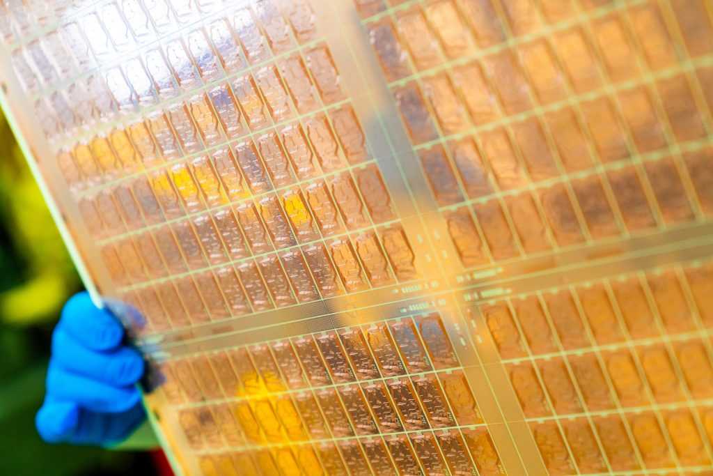
Materiali in vetro substrati del pacchetto rappresentano un progresso significativo nella tecnologia di confezionamento elettronico. Questi substrati, fatto di vetro, offrono numerosi vantaggi rispetto ai materiali tradizionali come il silicio o i substrati organici. Le loro proprietà uniche li rendono ideali per un'ampia gamma di applicazioni, comprese le alte frequenze, ad alta velocità, e dispositivi elettronici ad alta affidabilità.
Che cos'è un substrato del pacchetto di materiali in vetro?
Un substrato per imballaggi in materiali di vetro è un tipo di substrato per imballaggi elettronici realizzato in vetro. Questi substrati vengono utilizzati per supportare e collegare circuiti integrati (circuiti integrati) nei dispositivi elettronici. I substrati di vetro offrono un'elettricità superiore, meccanico, e proprietà termiche rispetto ai materiali convenzionali, rendendoli un'opzione interessante per applicazioni elettroniche avanzate.
Costante dielettrica elevata: Bicchiere substrati hanno una costante dielettrica elevata, che migliora l'integrità del segnale e riduce la perdita di segnale nelle applicazioni ad alta frequenza.
Stabilità termica: I materiali in vetro garantiscono un'eccellente stabilità termica, consentendo prestazioni affidabili in ambienti ad alta temperatura.
Resistenza meccanica: La resistenza e la rigidità intrinseche dei substrati di vetro migliorano la stabilità meccanica del dispositivo confezionato.
Guida di riferimento alla progettazione per substrati di confezioni di materiali in vetro
La progettazione dei substrati dei contenitori in materiali di vetro prevede diversi passaggi critici per garantire prestazioni e affidabilità ottimali.
La selezione del tipo appropriato di vetro è fondamentale per ottenere l'effetto elettrico desiderato, termico, e proprietà meccaniche. I materiali di vetro comuni utilizzati includono:
Vetro alluminosilicato: Noto per la sua elevata resistenza e stabilità termica.
Vetro borosilicato: Offre un'eccellente resistenza termica e chimica.
Vetro al quarzo: Fornisce un isolamento elettrico superiore e una perdita di segnale minima.
I substrati del pacchetto di materiali in vetro sono generalmente costituiti:
Strato centrale: Lo strato isolante centrale che fornisce integrità strutturale.
Strati di accumulo: Ulteriori strati aggiunti al nucleo per aumentare la densità di instradamento e migliorare le prestazioni elettriche.
Strati superficiali: Gli strati più esterni che includono le zone di contatto per la connessione a circuiti esterni.
Una gestione termica efficace è essenziale per mantenere le prestazioni e la longevità dei circuiti integrati. Le tecniche includono:
Vie termiche: Percorsi conduttivi che trasferiscono il calore dal circuito integrato al dissipatore di calore.
Diffusori di calore: Strati o componenti metallici che aiutano a distribuire e dissipare il calore.
Materiali di interfaccia termica (TIM): Materiali posizionati tra il circuito integrato e il diffusore di calore per migliorare la conduttività termica.
Garantire le prestazioni elettriche implica mantenere un'impedenza controllata, riducendo al minimo la perdita di segnale, e riducendo la diafonia. Ciò richiede:
Routing di traccia di precisione: Progettazione attenta delle larghezze delle tracce e della spaziatura per controllare l'impedenza.
Piani terrestri: Strati dedicati alla messa a terra per ridurre il rumore e migliorare l'integrità del segnale.
Schermatura: Tecniche per schermare segnali sensibili dalle interferenze elettromagnetiche.
Spessore del pannello: Determinato dal numero di strati e dai requisiti di progettazione generali.
Praticare fori e vie: Foratura precisa di fori e vie per connessioni tra strati.
Posizionamento dei componenti: Posizionamento strategico dei componenti per garantire facilità di test e risultati accurati.
Quali materiali vengono utilizzati nei substrati degli imballaggi in materiali di vetro?
I materiali utilizzati nei substrati dei pacchetti di materiali in vetro sono selezionati per le loro proprietà elettriche superiori, termico, e proprietà meccaniche. I materiali comuni includono:
Vetro alluminosilicato: Noto per la sua elevata resistenza e stabilità termica, il vetro alluminosilicato viene spesso utilizzato in applicazioni che richiedono robuste proprietà meccaniche.
Vetro borosilicato: Offre un'eccellente resistenza termica e chimica, il vetro borosilicato è adatto per ambienti ad alta temperatura e chimicamente aggressivi.
Vetro al quarzo: Con isolamento elettrico superiore e perdita di segnale minima, il vetro al quarzo è ideale per applicazioni ad alta frequenza.
Rame: Indispensabile per le piste e i pad conduttivi, il rame fornisce un'eccellente conduttività elettrica ed è ampiamente utilizzato negli strati superficiali e di accumulo.
Sfere di saldatura: Tipicamente realizzato con leghe saldanti senza piombo, queste sfere forniscono i collegamenti elettrici e meccanici tra il substrato e la scheda madre.
Di quali dimensioni sono i substrati del pacchetto di materiali in vetro?
Le dimensioni dei substrati dei contenitori in materiali di vetro possono variare ampiamente a seconda del circuito integrato specifico e dell'applicazione prevista. I fattori che influenzano la dimensione includono:
Dimensioni della matrice e numero di pin: La dimensione del die del circuito integrato e il numero di connessioni richieste influenzano la dimensione complessiva del substrato. I circuiti integrati ad alte prestazioni con die più grandi e più pin richiedono generalmente substrati più grandi.
Requisiti dell'applicazione: Diverse applicazioni, come il desktop, server, o CPU mobili, hanno vincoli dimensionali e requisiti prestazionali variabili che influiscono sulle dimensioni del substrato.
Standard di produzione: Anche gli standard di settore e le capacità produttive svolgono un ruolo nel determinare la dimensione dei substrati delle confezioni in materiali di vetro. Mentre ci sono dimensioni standard, è possibile progettare dimensioni personalizzate per applicazioni specifiche.
Il processo di produzione dei substrati per imballaggi in materiali di vetro
Il processo di produzione dei substrati degli imballaggi in materiali di vetro prevede diverse fasi precise e controllate:
Progettazione CAD: Vengono creati modelli CAD dettagliati, incorporando tutti gli strati, tracce, e componenti.
Simulazione: Vengono condotte simulazioni elettromagnetiche e termiche per ottimizzare il progetto e garantire che soddisfi i requisiti prestazionali.
Laminazione: Più strati di materiali isolanti e conduttivi vengono laminati insieme per formare il substrato.
Foratura e placcatura: I passaggi vengono perforati attraverso gli strati e placcati con rame per stabilire collegamenti elettrici.
Fotoincisione: Lo schema circuitale viene trasferito sul substrato mediante tecniche di fotoincisione, che comportano l'applicazione di un fotoresist, esponendolo ai raggi UV attraverso una maschera, e incidendo via le aree non protette.
Placcatura: Le tracce e i cuscinetti conduttivi sono placcati con rame aggiuntivo per migliorare le prestazioni elettriche.
Posizionamento della sfera di saldatura: Le sfere di saldatura vengono posizionate con precisione sul lato inferiore del substrato utilizzando apparecchiature automatizzate.
Saldatura a rifusione: Il substrato viene sottoposto a saldatura a riflusso per sciogliere e solidificare le sfere di saldatura, creando robuste connessioni elettriche e meccaniche.
Test elettrici: Vengono condotti rigorosi test elettrici per garantire che tutte le connessioni siano intatte e che il substrato funzioni come previsto.
Test termici: I test termici verificano la capacità del substrato di dissipare il calore e mantenere le prestazioni in condizioni operative.
Ispezione finale: Un'ispezione approfondita garantisce che il supporto soddisfi tutte le specifiche di progettazione e gli standard di qualità.
L'area di applicazione dei substrati per imballaggi in materiali di vetro
I substrati dei contenitori in materiali di vetro vengono utilizzati in una varietà di applicazioni in cui prestazioni elevate e affidabilità sono cruciali:
Elettronica di consumo: Utilizzato nelle CPU desktop e laptop, questi substrati supportano il calcolo ad alte prestazioni nei dispositivi di uso quotidiano.
Data Center e Server: I substrati CPU ad alte prestazioni sono essenziali per le applicazioni server e data center, dove affidabilità e prestazioni sono fondamentali.
Dispositivi mobili: Substrati CPU più piccoli ed efficienti vengono utilizzati negli smartphone e nei tablet per supportare il mobile computing ad alte prestazioni.
Sistemi integrati: Questi substrati si trovano anche nei sistemi embedded, fornire potenza di elaborazione per l'industria, automobilistico, e applicazioni IoT.
Calcolo ad alte prestazioni (HPC): Utilizzato nei sistemi HPC, questi substrati supportano i compiti computazionali più impegnativi, come simulazioni scientifiche e analisi dei dati.
Quali sono i vantaggi dei substrati per imballaggi in materiali di vetro?
I substrati dei contenitori in materiali di vetro offrono numerosi vantaggi che li rendono adatti per applicazioni informatiche ad alte prestazioni:
Prestazioni elettriche migliorate: Il design multistrato e il routing di precisione garantiscono prestazioni elettriche superiori, riducendo al minimo la perdita di segnale e la diafonia.
Gestione termica migliorata: Materiali avanzati e tecniche di gestione termica aiutano a dissipare il calore in modo efficace, mantenendo le prestazioni e l'affidabilità del circuito integrato.
Design compatto ed efficiente: L'uso di sfere di saldatura e componenti incorporati consente un design più compatto ed efficiente, risparmiare spazio sulla scheda madre.
Durata e affidabilità: Materiali di alta qualità e processi di produzione rigorosi garantiscono che questi substrati siano durevoli e affidabili, anche in condizioni impegnative.
Personalizzazione: La capacità di creare progetti personalizzati consente soluzioni su misura che soddisfano requisiti applicativi specifici, garantendo prestazioni ottimali.
Domande frequenti
Quali sono i principali vantaggi derivanti dall'utilizzo di substrati di package in materiali di vetro nel calcolo ad alte prestazioni?
I substrati dei contenitori in materiali di vetro forniscono prestazioni elettriche migliorate, gestione termica migliorata, design compatto ed efficiente, durabilità, affidabilità, e personalizzazione, rendendoli ideali per applicazioni informatiche ad alte prestazioni.
Come vengono fissate le sfere di saldatura ai substrati delle confezioni di materiali in vetro?
Le sfere di saldatura vengono posizionate sul lato inferiore del substrato utilizzando apparecchiature automatizzate e quindi saldate a riflusso per creare robuste connessioni elettriche e meccaniche.
Quali materiali sono comunemente utilizzati nei substrati degli imballaggi in materiali di vetro?
I materiali comuni includono il vetro alluminosilicato, vetro borosilicato, vetro al quarzo, rame per strati conduttivi, sfere di saldatura per i collegamenti, e vari materiali isolanti e protettivi.
In quali settori sono più comunemente utilizzati i substrati per imballaggi in materiali di vetro?
I substrati dei contenitori in materiali di vetro sono comunemente utilizzati nell'elettronica di consumo, data center e server, dispositivi mobili, sistemi integrati, e calcolo ad alte prestazioni.
In che modo i substrati degli imballaggi in materiali di vetro migliorano la gestione termica?
I substrati dei contenitori in materiali di vetro migliorano la gestione termica attraverso l'uso di canali termici, diffusori di calore, e materiali ad alte prestazioni che migliorano la dissipazione del calore e mantengono le prestazioni del dispositivo durante i test.