CO.,LTD")
Produttore di substrati FC-BGA multi-chip. Come multi-chip leader Substrati FC-BGA Produttore, siamo specializzati nella produzione ad alta densità, substrati ad alte prestazioni che consentono l'integrazione perfetta di più chip. I nostri processi di produzione avanzati e i rigorosi controlli di qualità garantiscono affidabilità ed efficienza, soddisfare le esigenti esigenze dell'elettronica moderna, compreso il calcolo ad alte prestazioni, telecomunicazioni, e data center.
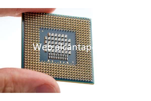
Matrice di griglie multi-chip Flip Chip Ball (FC-BGA) Substrati sono soluzioni di packaging avanzate che supportano l'integrazione di più chip semiconduttori in un unico package. Questi substrati sono fondamentali nel calcolo ad alte prestazioni, telecomunicazioni, ed elettronica avanzata, dove lo spazio, prestazione, e l'affidabilità sono fondamentali. Fornendo una piattaforma per più chip, I substrati FC-BGA consentono livelli di funzionalità più elevati, migliore gestione termica, e prestazioni elettriche migliorate.
Cos'è un substrato FC-BGA multi-chip?
Un substrato FC-BGA multichip è un tipo di packaging per semiconduttori che incorpora più chip su un singolo substrato utilizzando la tecnologia flip-chip. Questo metodo di confezionamento prevede di capovolgere i chip e di fissarli al substrato mediante protuberanze di saldatura, che forniscono collegamenti elettrici e supporto meccanico. Il substrato stesso è progettato per interconnettere i chip e gestire la distribuzione dell'energia, instradamento del segnale, e dissipazione termica.
Integrazione di più chip: Il vantaggio principale dei substrati FC-BGA multichip è la capacità di integrare diversi chip in un unico pacchetto. Questa integrazione consente sistemi elettronici più complessi e potenti riducendo l'ingombro complessivo.
Tecnologia Flip-Chip: La tecnologia Flip-chip prevede il fissaggio del lato attivo del die del semiconduttore al substrato. Questo metodo riduce al minimo la lunghezza delle interconnessioni, riducendo l’induttanza e la capacità parassita, che migliora l'integrità del segnale e le prestazioni elettriche.
Matrice di griglie di sfere (BGA) Disposizione: Il layout BGA prevede una fitta serie di sfere di saldatura sul lato inferiore del substrato, facilitando le interconnessioni ad alta densità con il circuito stampato (PCB). Questo layout supporta un robusto attacco meccanico e collegamenti elettrici affidabili.
Guida di riferimento alla progettazione per substrati FC-BGA multichip
La progettazione di substrati FC-BGA multichip implica diverse considerazioni chiave per garantire prestazioni ottimali, affidabilità, e producibilità:
Selezione dei materiali: La scelta dei materiali è fondamentale per i substrati FC-BGA multi-chip. Substrati organici o ceramici ad alte prestazioni vengono spesso utilizzati grazie alle loro eccellenti proprietà elettriche e termiche. I materiali devono inoltre offrire una buona stabilità meccanica e compatibilità con i processi flip-chip.
Progettazione del substrato: La progettazione del substrato deve accogliere più chip e fornire le interconnessioni necessarie. Ciò include un'attenta pianificazione dei livelli di routing, reti di distribuzione elettrica, e vie termiche per garantire prestazioni efficienti e affidabilità.
Gestione termica: Una gestione termica efficace è fondamentale nei substrati FC-BGA multichip. Ciò può comportare l'uso di vias termici, dissipatori di calore incorporati, e altre tecniche per dissipare in modo efficiente il calore generato dai chip multipli. È possibile utilizzare strumenti di simulazione avanzati per modellare il comportamento termico e ottimizzare la progettazione.
Integrità del segnale: Il mantenimento dell'integrità del segnale nelle applicazioni ad alta frequenza richiede un'attenzione particolare all'instradamento delle tracce, il posizionamento dei componenti, e il design del substrato. Tecniche come il routing ad impedenza controllata, instradamento di coppie differenziali, e la schermatura può essere impiegata per ridurre al minimo la degradazione del segnale.
Producibilità: La progettazione deve considerare la producibilità per garantire che il substrato possa essere prodotto in modo affidabile ed economicamente vantaggioso. Ciò include considerazioni per il processo di fabbricazione, processo di assemblaggio, e requisiti di prova.
Quali materiali vengono utilizzati nei substrati FC-BGA multichip?
I materiali utilizzati nei substrati FC-BGA multichip sono selezionati in base alla loro elettricità, termico, e proprietà meccaniche. I materiali primari includono:
Substrati organici: Substrati organici ad alte prestazioni, come quelli realizzati in resina epossidica o BT (bismaleimide triazina) resina, sono comunemente usati. Questi materiali forniscono un buon isolamento elettrico, stabilità termica, e resistenza meccanica.
Substrati ceramici: Substrati ceramici, come l'allumina o il nitruro di alluminio, sono utilizzati per applicazioni che richiedono conduttività termica e stabilità meccanica superiori. Questi materiali sono ideali per applicazioni ad alta potenza e ad alta frequenza.
Rame: Il rame viene utilizzato per le tracce e i cuscinetti conduttivi sul substrato. La sua eccellente conduttività elettrica lo rende ideale per formare percorsi elettrici e interconnessioni tra i chip e il PCB.
Dossi di saldatura: Per fissare i chip semiconduttori al substrato vengono utilizzati rilievi di saldatura realizzati con leghe senza piombo. Questi dossi forniscono collegamenti elettrici e supporto meccanico.
Che dimensioni hanno i substrati FC-BGA multi-chip?
Le dimensioni dei substrati FC-BGA multichip possono variare ampiamente a seconda dell'applicazione e dei requisiti di progettazione:
Dimensioni standard: I substrati FC-BGA multichip possono essere prodotti in dimensioni standard, come 35 mm x 35 mm o 40 mm x 40 mm. Queste dimensioni sono comunemente utilizzate nella produzione su larga scala e possono essere personalizzate per adattarsi ad applicazioni specifiche.
Dimensioni personalizzate: Per applicazioni specializzate, I substrati FC-BGA multichip possono essere prodotti in dimensioni e forme personalizzate. Questa flessibilità consente ai progettisti di ottimizzare la disposizione del substrato per chip e sistemi specifici.
Spessore: Anche lo spessore dei substrati multi-chip FC-BGA può variare, tipicamente vanno da 0,5 mm a 1,5 mm o più. Lo spessore è influenzato dal numero di strati, la progettazione del percorso, e i requisiti di gestione termica.
Il processo di produzione di substrati FC-BGA multi-chip
Il processo di produzione dei substrati FC-BGA multichip prevede diverse fasi precise e controllate per garantire qualità e prestazioni elevate:
Progettazione e prototipazione: Il processo inizia con la progettazione dettagliata e la prototipazione. Gli ingegneri creano un diagramma schematico e un layout del substrato, considerando il posizionamento dei chip e l'instradamento delle interconnessioni. La prototipazione consente di testare e perfezionare il design.
Fabbricazione del substrato: Una volta finalizzato il progetto, il substrato è fabbricato. Ciò comporta:
Impilamento di strati: Strati multipli di materiali conduttivi e isolanti sono impilati e incollati insieme.
Attraverso la formazione: All'interno degli strati vengono formati dei passaggi per creare connessioni elettriche tra i diversi strati. Queste vie possono essere forate utilizzando tecniche laser o meccaniche.
Acquaforte e placcatura: Sugli strati sono incise tracce conduttive, e i vias sono placcati per formare i percorsi elettrici.
Formazione di cavità: Se necessario, all'interno del substrato si formano cavità per ospitare componenti specifici o funzionalità di gestione termica.
Attacco per chip: I chip semiconduttori sono fissati al substrato mediante la tecnologia flip-chip:
Urtare: Sul lato attivo dei chip vengono depositati rilievi di saldatura.
Incollaggio Flip-Chip: I chip vengono capovolti e fissati al substrato utilizzando un processo che allinea le protuberanze di saldatura con i corrispondenti pad sul substrato.
Saldatura a rifusione: L'assieme viene riscaldato per sciogliere le protuberanze di saldatura, creando forti connessioni meccaniche ed elettriche tra i chip e il substrato.
Assemblaggio di componenti: Componenti aggiuntivi, come dispositivi passivi o cappucci protettivi, sono assemblati sul substrato utilizzando la tecnologia di montaggio superficiale (SMT) o altre tecniche.
Test e controllo qualità: Test rigorosi e controlli di qualità garantiscono che i substrati soddisfino le specifiche di progettazione e gli standard prestazionali. Ciò include:
Test elettrici: I substrati vengono testati per garantire che funzionino correttamente e soddisfino i requisiti di prestazione elettrica.
Test termici: I substrati sono sottoposti a test termici per garantire che possano dissipare efficacemente il calore e mantenere le prestazioni in varie condizioni.
Ispezione finale: Un'ispezione finale verifica che i substrati siano privi di difetti e pronti per la distribuzione.
L'area di applicazione dei substrati FC-BGA multichip
I substrati FC-BGA multichip sono utilizzati in un'ampia gamma di applicazioni ad alte prestazioni grazie al loro design e alle loro capacità unici:
Informatica ad alte prestazioni: Nel calcolo ad alte prestazioni, I substrati FC-BGA multichip vengono utilizzati nei processori, GPU, e altri componenti critici. La loro capacità di integrare più chip in un unico pacchetto aumenta la potenza e l'efficienza computazionali.
Telecomunicazioni: Nelle telecomunicazioni, questi substrati sono utilizzati nelle stazioni base, ricetrasmettitori, e altre applicazioni RF e microonde. The improved thermal management and signal integrity of Multi-Chip FC-BGA Substrates enhance the performance and reliability of telecommunications systems.
Aerospaziale e Difesa: I substrati multi-chip FC-BGA sono utilizzati nell'avionica, sistemi radar, e altri dispositivi elettronici ad alte prestazioni nei settori aerospaziale e della difesa. La loro capacità di ospitare componenti elettronici complessi in una forma compatta e leggera è fondamentale per queste applicazioni.
Dispositivi medici: Questi substrati vengono utilizzati in dispositivi medici come apparecchiature per l'imaging, strumenti diagnostici, e monitor sanitari indossabili. Le loro dimensioni compatte e le prestazioni affidabili sono essenziali per la precisione e l'affidabilità richieste nelle applicazioni mediche.
Elettronica automobilistica: I substrati multi-chip FC-BGA sono impiegati in sistemi avanzati di assistenza alla guida (ADAS), sistemi di infotainment, e altri componenti elettronici automobilistici. La loro capacità di integrare molteplici funzioni in un fattore di forma compatto è particolarmente preziosa nei veicoli moderni.
Quali sono i vantaggi dei substrati FC-BGA multi-chip?
I substrati FC-BGA multichip offrono numerosi vantaggi che li rendono essenziali per le applicazioni elettroniche ad alte prestazioni:
Alta densità di integrazione: Integrando più chip in un unico pacchetto, I substrati FC-BGA multichip consentono livelli più elevati di funzionalità e prestazioni riducendo l'ingombro complessivo.
Gestione termica migliorata: La capacità di incorporare vias termici, dissipatori di calore, e altre funzionalità di gestione termica all'interno del substrato consentono un'efficiente dissipazione del calore. Ciò migliora le prestazioni e l'affidabilità dei componenti ad alta potenza.
Prestazioni elettriche migliorate: La tecnologia flip-chip e la stretta vicinanza dei componenti all'interno del substrato migliorano l'integrità del segnale e riducono la lunghezza delle interconnessioni. Ciò porta a una minore induttanza e capacità parassita, che è vantaggioso per le applicazioni ad alta frequenza.
Maggiore affidabilità: Il design integrato dei substrati FC-BGA multichip riduce il numero di giunti di saldatura e di interconnessioni, che possono essere potenziali punti di fallimento. Ciò migliora l’affidabilità complessiva del sistema elettronico.
Compatto e leggero: La capacità di integrare più chip e componenti in un unico pacchetto riduce le dimensioni e il peso complessivi del sistema elettronico. Ciò è particolarmente vantaggioso nelle applicazioni
Domande frequenti
Quali sono le considerazioni chiave nella progettazione di un substrato FC-BGA multi-chip??
Le considerazioni chiave includono la selezione del materiale, progettazione del substrato, gestione termica, Integrità del segnale, e producibilità. Questi fattori devono essere attentamente bilanciati per garantire prestazioni ottimali, affidabilità, ed efficienza in termini di costi.
In che modo i substrati FC-BGA multichip migliorano la gestione termica?
I substrati FC-BGA multichip migliorano la gestione termica incorporando vie termiche, dissipatori di calore, e altre funzionalità di gestione termica all'interno del substrato. Questi elementi di progettazione consentono un'efficiente dissipazione del calore dai componenti ad alta potenza, mantenendo prestazioni e affidabilità.
Quali applicazioni traggono maggiori vantaggi dai substrati FC-BGA multichip?
Le applicazioni che traggono maggiori vantaggi dai substrati FC-BGA multichip includono il calcolo ad alte prestazioni, telecomunicazioni, aerospaziale e della difesa, dispositivi medici, ed elettronica automobilistica. Questi substrati supportano sistemi elettronici complessi e potenti riducendo al contempo dimensioni e peso.
Quali materiali sono comunemente utilizzati nei substrati FC-BGA multichip?
I materiali comuni includono substrati organici ad alte prestazioni (come resina epossidica o BT), substrati ceramici (come l'allumina o il nitruro di alluminio), rame per tracce conduttive, e protuberanze di saldatura senza piombo per il fissaggio del chip.
In che modo la tecnologia flip-chip migliora le prestazioni dei substrati FC-BGA multi-chip?
La tecnologia Flip-chip migliora le prestazioni riducendo al minimo la lunghezza delle interconnessioni, riducendo l’induttanza e la capacità parassita. Ciò migliora l'integrità del segnale e le prestazioni elettriche, rendendolo ideale per applicazioni ad alta frequenza e ad alta potenza.