المحدودة")
الركيزة الزجاجية لمصنع أشباه الموصلات., فقدان عازلة منخفضة, والوضوح البصري العالي. هذه الميزات تجعلها مثالية لتطبيقات أشباه الموصلات المتقدمة, بما في ذلك الصور الضوئية ولوحات العرض. يمكّن سطحهم الأمل, تلبية متطلبات الالكترونيات الحديثة.
ظهرت ركائز الزجاج كمواد حاسمة في صناعة أشباه الموصلات, تقدم خصائص فريدة مناسبة تمامًا للتطبيقات المتقدمة. يتم استخدام هذه الركائز بشكل متزايد في أجهزة أشباه الموصلات المختلفة نظرًا لاستقرارها الحراري الممتاز, ثابت عازل منخفض, ومقاومة كيميائية عالية. زجاج ركائز توفير أساس موثوق لتصنيع أجهزة أشباه الموصلات, تمكين تطوير أصغر, أسرع, ومكونات إلكترونية أكثر كفاءة.
ما هي الركيزة الزجاجية لأشباه الموصلات?
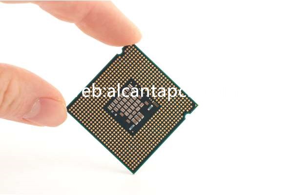
الركيزة الزجاجية لأشباه الموصلات رقيقة, قطعة مسطحة من الزجاج تستخدم كمادة أساسية لتصنيع أجهزة أشباه الموصلات. على عكس الركائز التقليدية المصنوعة من السيليكون أو مواد أخرى, توفر الركائز الزجاجية العديد من المزايا, بما في ذلك الشفافية البصرية العالية, استقرار حراري وكيميائي ممتاز, والقدرة على دعم الزخرفة الدقيقة المطلوبة لأجهزة أشباه الموصلات المتقدمة. هذه الخصائص تجعل الزجاج مادة مثالية لمجموعة واسعة من تطبيقات أشباه الموصلات, بما في ذلك الدوائر المتكاملة, أجهزة استشعار, وتقنيات العرض.
تُصنع الركائز الزجاجية عادة من مواد عالية النقاء مثل البورسليكات أو السيليكا المنصهرة, والتي توفر خصائص حرارية وميكانيكية استثنائية. يتم تصنيع هذه الركائز لتكون مسطحة للغاية وسلسة, مع قياس خشونة السطح بالنانومتر, ضمان الترسيب الدقيق لمواد أشباه الموصلات أثناء تصنيع الجهاز.
في سياق تصنيع أشباه الموصلات, غالبًا ما تستخدم الركائز الزجاجية في إنتاج الترانزستورات ذات الأغشية الرقيقة (TFTs), الأنظمة الكهروميكانيكية الدقيقة (ممس), وغيرها من الأجهزة التي تتطلب دقة وثبات عاليين. كما أن شفافية الركائز الزجاجية تجعلها خيارًا ممتازًا للتطبيقات التي تتضمن مكونات بصرية, مثل الأجهزة الضوئية وشاشات العرض المتقدمة.
المواد وخصائص ركائز الزجاج
عادة ما يتم تصنيع الركائز الزجاجية لأشباه الموصلات من مجموعة متنوعة من أنواع الزجاج المتخصصة, يقدم كل منها خصائص فريدة تلبي احتياجات تطبيقات أشباه الموصلات المختلفة. المواد الأكثر استخدامًا تشمل زجاج البورسليكات, زجاج الألومينوسيليكات, والسيليكا المنصهرة.
هذا النوع من الزجاج معروف بثباته الحراري الممتاز ومعامل التمدد الحراري المنخفض. إنه مقاوم للغاية للصدمات الحرارية والتآكل الكيميائي, مما يجعلها مناسبة للتطبيقات التي تكون فيها تقلبات درجات الحرارة شائعة.
يُقدر زجاج الألومنيوم سيليكات بقوته الميكانيكية ومتانته. لديه معامل تمدد حراري أعلى من زجاج البورسليكات, ولكنها توفر مقاومة فائقة للخدش والتأثير, مما يجعلها مثالية للطبقات الواقية في أجهزة أشباه الموصلات.
السيليكا المنصهرة عالية النقاء, زجاج صناعي يوفر وضوحًا بصريًا استثنائيًا وتمددًا حراريًا منخفضًا. ويستخدم عادة في التطبيقات التي تتطلب دقة عالية, مثل أقنعة الطباعة الحجرية الضوئية والمكونات البصرية في أجهزة أشباه الموصلات.
خصائص هذه الركائز الزجاجية تجعلها مناسبة للغاية للاستخدام في تصنيع أشباه الموصلات:
يمكن للركائز الزجاجية أن تتحمل درجات الحرارة العالية دون تشويه أو فقدان سلامتها الهيكلية, وهو أمر ضروري أثناء عمليات الترسيب والتليين في تصنيع أشباه الموصلات.
انخفاض ثابت العزل الكهربائي للزجاج الركيزة يساعد على تقليل فقدان الإشارة والتحدث المتبادل في التطبيقات عالية التردد, مما يجعلها مثالية للاستخدام في أجهزة الترددات اللاسلكية والميكروويف.
ركائز الزجاج مقاومة للغاية للأحماض, القلويات, وغيرها من المواد الكيميائية المستخدمة عادة في معالجة أشباه الموصلات, ضمان الموثوقية والمتانة على المدى الطويل.
تسمح شفافية الركائز الزجاجية بدمج المكونات البصرية, مما يجعلها مناسبة للأجهزة الإلكترونية البصرية وتقنيات العرض المتقدمة.
عملية تصنيع الركائز الزجاجية لأشباه الموصلات
تتضمن عملية تصنيع الركائز الزجاجية لأشباه الموصلات عدة خطوات رئيسية مصممة لإنتاج جودة عالية, ركائز مسطحة للغاية مناسبة لتطبيقات أشباه الموصلات المتقدمة:
تبدأ العملية باختيار المواد الخام عالية النقاء, مثل السيليكا, الألومينا, وغيرها من الإضافات, اعتمادا على الخصائص المطلوبة للزجاج. ويتم صهر هذه المواد عند درجات حرارة عالية في الفرن لتكوين زجاج منصهر متجانس.
يتم بعد ذلك تشكيل الزجاج المنصهر إلى صفائح أو ألواح باستخدام تقنيات مثل الزجاج المصقول أو رسم الانصهار. في عملية الزجاج المصقول, يطفو الزجاج المنصهر على طبقة من القصدير المنصهر, حيث ينتشر إلى رقيقة, ورقة مسطحة. في عملية رسم الانصهار, يتم سحب الزجاج المنصهر عموديًا من البوتقة, إنتاج صفائح مسطحة وناعمة للغاية.
بعد التشكيل, يتم تبريد الألواح الزجاجية ببطء في فرن التلدين لتخفيف الضغوط الداخلية وتحسين قوتها الميكانيكية. هذه الخطوة حاسمة لضمان استقرار الأبعاد للركائز الزجاجية أثناء المعالجة اللاحقة.
يتم بعد ذلك صقل الألواح الزجاجية لتحقيق النعومة والتسطيح المطلوبين للسطح. يتضمن ذلك مراحل متعددة من الطحن والتلميع, في كثير من الأحيان باستخدام التلميع الكيميائي والميكانيكي (CMP) التقنيات. عادة ما تكون خشونة السطح النهائية في نطاق النانومتر, وهو أمر بالغ الأهمية للترسيب الدقيق للمواد أشباه الموصلات.
تخضع الركائز الزجاجية النهائية لفحص صارم للتأكد من أنها تلبي المتطلبات الصارمة لصناعة أشباه الموصلات. وهذا يشمل قياس سمك, التسطيح, خشونة السطح, والتفتيش عن أي عيوب مثل الخدوش, الادراج, أو فقاعات.
يتم قطع ركائز الزجاج إلى الحجم والشكل المطلوب, ثم يتم تعبئتها بعناية لمنع التلوث أو التلف أثناء النقل والتخزين.
تطبيقات ركائز الزجاج في أشباه الموصلات
تُستخدم الركائز الزجاجية في مجموعة واسعة من تطبيقات أشباه الموصلات نظرًا لخصائصها الفريدة. وتشمل بعض التطبيقات الرئيسية:
تستخدم ركائز الزجاج على نطاق واسع في إنتاج TFTs, وهي مكونات أساسية في شاشات العرض المسطحة مثل شاشات LCD وشاشات OLED. إن شفافية الزجاج وثباته تجعله مادة مثالية لهذه التطبيقات.
أجهزة ممس, مثل أجهزة الاستشعار والمحركات, غالبًا ما تستخدم ركائز زجاجية نظرًا لخصائصها الحرارية والميكانيكية الممتازة. تعد دقة الزجاج وثباته أمرًا بالغ الأهمية للتشغيل الدقيق لهذه الأجهزة المصغرة.
تُستخدم الركائز الزجاجية بشكل شائع في الأجهزة الضوئية, بما في ذلك أدلة الموجات, المغيرون, والكاشفات الضوئية. تسمح الشفافية البصرية للزجاج بنقل الضوء ومعالجته بكفاءة, وهو أمر ضروري في هذه التطبيقات.
في عبوات أشباه الموصلات المتقدمة, تُستخدم الركائز الزجاجية كوسطاء وحاملات لدمج العديد من المرحلية في حزمة واحدة. يساعد استقرار الأبعاد وثابت العزل الكهربائي المنخفض للزجاج على تحسين سلامة الإشارة وتقليل التأثيرات الطفيلية في العبوات عالية الكثافة.
مزايا الركائز الزجاجية في أشباه الموصلات
يوفر استخدام الركائز الزجاجية في أشباه الموصلات العديد من المزايا, المساهمة في أداء وموثوقية أجهزة أشباه الموصلات:
توفر الركائز الزجاجية منصة مستقرة ودقيقة لتصنيع أجهزة أشباه الموصلات, ضمان أداء ثابت عبر مجموعة واسعة من ظروف التشغيل.
تساعد الخصائص الحرارية الممتازة للركائز الزجاجية على إدارة تبديد الحرارة في أجهزة أشباه الموصلات عالية الطاقة, تقليل مخاطر الفشل الناجم عن الحرارة.
يقلل ثابت العزل الكهربائي المنخفض للركائز الزجاجية من فقدان الإشارة والتحدث المتبادل, مما يجعلها مثالية للتطبيقات عالية التردد في أجهزة الترددات اللاسلكية والميكروويف.
تسمح شفافية الركائز الزجاجية بدمج المكونات البصرية, تمكين تطوير الأجهزة الإلكترونية الضوئية المتقدمة وشاشات العرض.
التعليمات
ما هي المواد الأولية المستخدمة في ركائز الزجاج لأشباه الموصلات?
تشمل المواد الشائعة زجاج البورسليكات, زجاج الألومينوسيليكات, والسيليكا المنصهرة, يقدم كل منها خصائص فريدة مصممة خصيصًا لتطبيقات محددة لأشباه الموصلات.
لماذا يُفضل الزجاج على السيليكون في بعض تطبيقات أشباه الموصلات؟?
يقدم الزجاج مزايا مثل انخفاض ثابت العزل الكهربائي, شفافية بصرية أعلى, واستقرار حراري أفضل, مما يجعلها مناسبة للتطبيقات التي تكون فيها هذه الخصائص حاسمة.
هل يمكن استخدام الركائز الزجاجية في أجهزة أشباه الموصلات عالية التردد؟?
نعم, إن ثابت العزل الكهربائي المنخفض والثبات العالي للركائز الزجاجية يجعلها مثالية للتطبيقات عالية التردد, بما في ذلك أجهزة الترددات اللاسلكية والميكروويف.
ما هو الدور الذي تلعبه الركائز الزجاجية في عبوات أشباه الموصلات المتقدمة?
في عبوات متقدمة, يتم استخدام ركائز زجاجية كوسطاء وناقلات, توفير منصة مستقرة لدمج العديد من المرحلية وتحسين سلامة الإشارة في التغليف عالي الكثافة.