المحدودة")
الشركة المصنعة العالمية لركيزة أشباه الموصلات. نحن نستخدم تقنية Msap وSap المتقدمة لتصنيع ركائز حزمة التوصيل البيني عالية الطبقات.
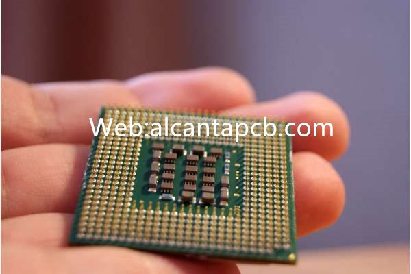
في عمليات تصميم وتصنيع المعدات الإلكترونية المعاصرة, ال الركيزة الحزمة يقف كمكون إلكتروني محوري. وتكمن وظيفتها الأساسية في دعم وربط رقائق أشباه الموصلات والعناصر الإلكترونية الأخرى. في الأساس, تعمل ركيزة الحزمة بمثابة “مؤسسة” من الأجهزة الإلكترونية, تقديم منصة للتكامل والتنسيق بين المكونات المتنوعة.
للتعمق أكثر في دورها, تعمل ركيزة الحزمة في المقام الأول على تسهيل الدعم والتوصيل البيني لرقائق أشباه الموصلات, المعالجات الشاملة, وحدات الذاكرة, أجهزة استشعار, وأكثر. من خلال هذا التكامل على حزمة الركيزة, يمكن لهذه الرقائق التواصل والتعاون مع المكونات الأخرى, وبالتالي تحقيق الوظائف المختلفة للأجهزة الإلكترونية. علاوة على ذلك, تتولى ركيزة الحزمة مسؤولية توزيع ونقل الطاقة الكهربائية والإشارات لضمان التشغيل السلس لجميع المكونات داخل الجهاز.
يؤكد التعقيد المتزايد للأجهزة الإلكترونية الحديثة على ضرورة ركائز الحزمة في مواجهة هذا التحدي. إنها تتيح دمج الرقائق المتنوعة ذات الوظائف المميزة في مساحة صغيرة, وبالتالي يؤدي إلى التكامل العالي وتصغير الأجهزة. على سبيل المثال, في الهاتف الذكي, تستوعب ركيزة الحزمة المعالجات, وحدات الذاكرة, رقائق الاتصالات, إلخ., دمجها بإحكام لتعزيز الكفاءة العامة واستقرار الجهاز.
فضلاً عن ذلك, من الأهمية بمكان النظر بدقة في التصميم واختيار المواد لركائز الحزمة. تحتاج هذه الركائز إلى إظهار التوصيل الحراري الممتاز والخصائص الكهربائية لضمان التشغيل السلس والتواصل بين الرقائق. في نفس الوقت, مع تزايد الطلب على الأجهزة الإلكترونية المدمجة وخفيفة الوزن, يجب أن تتمتع ركائز العبوة بالقوة والمتانة الكافية لتحمل الاستخدام اليومي والظروف البيئية المختلفة.
في الجوهر, تلعب ركائز الحزمة دورًا لا غنى عنه في الأجهزة الإلكترونية الحديثة. كمكون إلكتروني حاسم, فهي تسهل الدعم والتوصيل البيني لرقائق أشباه الموصلات والعناصر الإلكترونية المتنوعة, قيادة التكامل العالي, التصغير, والتشغيل الفعال للمعدات. خالية من ركائز الحزمة, ستفشل الأجهزة الإلكترونية الحديثة في تحقيق الوظائف المعقدة ومستويات الأداء التي تظهرها حاليًا.
ما هي أنواع ركيزة الحزمة التي تقدمها الشركات المصنعة لركيزة أشباه الموصلات?
في قطاع الالكترونيات المعاصرة, يحتل مصنعو الركيزة لأشباه الموصلات موقعًا محوريًا, توفير مجموعة من ركائز الحزمة المخصصة لسياقات التطبيقات المتنوعة. ومن بين الأنواع السائدة لوحات HDI (ربط عالي الكثافة) والألواح الصلبة المرنة.
إنهم يجدون فائدة في مجال الإلكترونيات التي تتطلب أداءً عاليًا وتصميمًا مضغوطًا, مثل الهواتف الذكية والأجهزة اللوحية. بسبب تصميمها المعقد والعمليات الصعبة, غالبًا ما يتطلب تصنيع لوحات HDI التعاون مع الشركات المصنعة المتخصصة لركائز أشباه الموصلات.
على الجانب الآخر, تجمع الألواح الصلبة المرنة بين ميزات الألواح الصلبة والمرنة, توفير قدرات الانحناء للاتصالات الموثوقة بين المكونات, مثالية للتطبيقات التي تتطلب مقاومة الاهتزاز والتأثير مثل المعدات الفضائية والطبية.
عند اختيار الركيزة الحزمة المناسبة, يعد تحديد المواصفات الفنية ومؤشرات الأداء بناءً على احتياجات المشروع أمرًا ضروريًا. على سبيل المثال, المشاريع التي تتطلب توصيلات كهربائية معقدة في المساحات الضيقة قد تفضل لوحات HDI, في حين أن تلك التي تتطلب المرونة وأداء الانحناء قد تميل نحو الألواح الصلبة المرنة. بالإضافة إلى ذلك, النظر في عمليات التصنيع والتكاليف أمر بالغ الأهمية.
في الأساس, توفر الشركات المصنعة العالمية لركيزة أشباه الموصلات العديد من ركائز الحزمة مثل HDI واللوحات الصلبة المرنة, تلبية متطلبات التطبيقات المتنوعة وتوسيع خيارات التصميم للأجهزة الإلكترونية. من خلال اتخاذ خيارات مستنيرة وتحسين التصاميم, يمكن للمنتجات الإلكترونية تحقيق أداء وموثوقية أفضل.
ما هي مزايا Package Substrate مقارنة بلوحات الدوائر التقليدية؟?
هذه المزايا مفصلة أدناه:
كثافة أعلى: تم تصميم Package Substrate لتكون أكثر إحكاما ويمكن أن تستوعب المزيد من المكونات الإلكترونية وخطوط الاتصال في نفس المنطقة. باستخدام تصميم التراص متعدد الطبقات وتكنولوجيا الدوائر الدقيقة, تحقق ركيزة الحزمة كثافة أعلى للجهاز, وبالتالي توفير مساحة أكبر لتوسيع وظيفة الجهاز.
سلامة إشارة أفضل: في حزمة الركيزة, الاتصالات بين عناصر الدائرة أقصر وأكثر إحكاما, تقليل طول مسار إرسال الإشارة وإمكانية عدم تطابق المعاوقة, وبالتالي تحسين سلامة الإشارة واستقرارها. فضلاً عن ذلك, باستخدام مواد وعمليات أكثر تقدما, يمكن أن تقلل ركيزة الحزمة من تداخل الإشارة والضوضاء وتحسين وضوح الإشارة ودقتها.
انخفاض التكاليف: في حين قد تكون هناك حاجة إلى الاستثمار الأولي والدعم الفني للتصنيع الأولي لركيزة الحزمة, العمليات طويلة الأجل تؤدي إلى تخفيضات في التكاليف. ويرجع ذلك إلى ارتفاع كثافة الجهاز وتحسين سلامة الإشارة في Package Substrate, السماح لمزيد من الوظائف في مساحة أصغر. بالتالي, هناك حاجة أقل للمكونات والملحقات الإضافية, مما يؤدي إلى توفير التكاليف الإجمالية.
تحسين كفاءة الإنتاج: تصميم مدمج لـ Package Substrate وآلي, تؤدي عمليات التصنيع القابلة للتطوير إلى تحسينات كبيرة في كفاءة الإنتاج. يتيح استخدام تقنيات التصنيع المتقدمة دورات إنتاج أسرع وزيادة الإنتاجية, تلبية متطلبات السوق الديناميكية ومتطلبات تسليم المنتجات العاجلة.
في ملخص, مقارنة بلوحات الدوائر التقليدية, توفر حزمة الركيزة مزايا متميزة في الكثافة, سلامة الإشارة, يكلف, وكفاءة الإنتاج. يمثل اعتمادها على نطاق واسع اتجاهًا حاسمًا في تصميم وتصنيع المعدات الإلكترونية الحديثة, تقديم فرص وتحديات جديدة لتطوير صناعة الإلكترونيات والابتكار.
ما هي عملية تصنيع الركيزة الحزمة?
تعتبر عملية تصنيع ركائز التغليف عملية دقيقة للغاية, وتتميز بالعديد من الإجراءات المعقدة والتقنيات المتطورة. يستخدم مصنعو ركائز أشباه الموصلات معدات وتقنيات متقدمة لضمان جودة وموثوقية منتجاتهم.
بدءًا, تبدأ العملية بالتصميم والتخطيط الهندسي, تشمل المهام مثل تحديد أبعاد اللوحة, عدد الطبقات, وتكوين الدائرة. بمجرد الانتهاء من مرحلة التصميم, تبدأ عمليات التصنيع.
المرحلة الأولى تنطوي على إعداد الركيزة, حيث يتم عادةً غمر قماش الألياف الزجاجية في الراتينج ومن ثم ضغطه إلى صفائح رقيقة تحت درجات حرارة وضغوط مرتفعة. تضمن هذه الخطوة الحاسمة متانة واستقرار الركيزة.
بعد إعداد الركيزة يتم تصنيع الدوائر المطبوعة (ثنائي الفينيل متعدد الكلور) عملية, والذي يستلزم تكوين آثار النحاس على الركيزة من خلال تقنيات مثل الطباعة الحجرية الضوئية والحفر. يتم أيضًا تنفيذ إجراءات إضافية مثل تنفيذ دوائر متعددة الطبقات وملء الفتحات النحاسية بأقصى قدر من الدقة باستخدام معدات متقدمة, ضمان دقة الخط والتوحيد لا تشوبها شائبة.
عند الانتهاء من تصنيع ثنائي الفينيل متعدد الكلور, تستلزم المرحلة اللاحقة تركيب الرقائق والمكونات الإلكترونية الأخرى. تتطلب هذه العملية استخدام آلات آلية متطورة لتحديد موضع الرقائق والمكونات وتوصيلها بدقة مع دوائر الركيزة. تعد دقة هذه العملية أمرًا بالغ الأهمية لضمان الأداء الأمثل للمنتج واستقراره.
تبعًا, يتم إجراء إجراءات التغليف والاختبار. خلال هذه المرحلة, يتم تغليف الركيزة داخل غلاف واقي وإخضاعها لمجموعة من الاختبارات للتحقق من مطابقتها لمعايير ومواصفات الجودة الصارمة. تشمل هذه الاختبارات تقييمات مختلفة مثل التقييمات الكهربائية, الفحوصات الوظيفية, واختبارات المرونة البيئية.
يستخدم مصنعو الركيزة لأشباه الموصلات مجموعة شاملة من تدابير مراقبة الجودة للحفاظ على جودة المنتج واستقراره. وتشمل هذه التدابير استخدام تقنيات التصوير والفحص المتقدمة لتحديد عيوب التصنيع, فضلا عن تنفيذ أنظمة إدارة الجودة الصارمة للإشراف على كل مرحلة من مراحل الإنتاج بعناية.
في أي المجالات يتم استخدام Package Substrate على نطاق واسع?
تعد Package Substrate مكونًا إلكترونيًا مهمًا يستخدم على نطاق واسع في صناعات متنوعة بما في ذلك الاتصالات, طبي, السيارات, وأكثر. ويفترض دورا محوريا في هذه المجالات, تسهيل الحلول المستقرة والموثوقة عبر سيناريوهات التطبيقات المختلفة من خلال التعاون مع المكونات الإلكترونية الأخرى.
في مجال الاتصالات, تعمل Package Substrate بمثابة العمود الفقري في توصيل المعلومات ونقلها. داخل أجهزة الاتصالات اللاسلكية مثل الهواتف المحمولة والمحطات القاعدية, تعمل ركيزة الحزمة على دعم المكونات وربطها مثل وحدات الترددات الراديوية, هوائيات, والمعالجات الدقيقة, ضمان النقل المستمر ومعالجة الإشارات. صفاته الكثافة العالية, تكرار, تعمل سلامة الإشارة على تمكين معدات الاتصالات من تحقيق نقل سريع وموثوق للبيانات, تلبية متطلبات المستخدم لسرعة الاتصال والجودة.
ضمن المجال الطبي, يتم استخدام Package Substrate على نطاق واسع في مجموعة من المعدات الطبية بما في ذلك أجهزة التصوير الطبي والأجهزة الطبية القابلة للزرع. التعاون مع مكونات مثل أجهزة الاستشعار ورقائق التحكم, فهو يسهل التحكم الدقيق والحصول على البيانات في المعدات الطبية. نظرا لمتطلبات الاستقرار والسلامة الصارمة للأجهزة الطبية, تظهر موثوقية واستقرار Package Substrate كعوامل محورية في ضمان التشغيل السلس والتشخيص الدقيق للمعدات الطبية.
يتيح تعاونها مع المكونات الإلكترونية الأخرى لسيناريوهات التطبيق المختلفة تحقيق وظائف مستقرة وموثوقة. كثافتها العالية, يضمن التردد العالي وسلامة الإشارة الممتازة أداء وموثوقية المعدات الإلكترونية, تقديم دعم مهم للحياة الحديثة والتنمية الصناعية.
كيفية العثور على حزمة الركيزة والحصول عليها?
عند البحث عن حزمة الركيزة والحصول عليها, تحتاج أولاً إلى تحديد المورد المناسب. فيما يلي بعض الخطوات والاقتراحات لمساعدتك في العثور على الشركة المصنعة العالمية المناسبة لركيزة أشباه الموصلات والحصول على عرض أسعار:
تحديد الاحتياجات: أولاً, توضيح احتياجاتك المحددة لركيزة الحزمة, بما في ذلك النوع, تحديد, كمية, إلخ. سيساعد ذلك في تضييق نطاق مجموعة الموردين والتأكد من أن المورد المختار سوف يلبي احتياجاتك.
البحث على الانترنت: استخدم موارد الإنترنت للبحث عن الشركات المصنعة العالمية لركائز أشباه الموصلات عبر الإنترنت. يمكنك العثور على العديد من الموردين المحتملين من خلال محركات البحث, مواقع صناعة الإلكترونيات المتخصصة وأدلة الموردين.
فحص الموردين: تصفية نتائج البحث واختيار العديد من الموردين ذوي السمعة الجيدة والقدرات المهنية. التركيز على مجموعة منتجاتهم, القدرة الإنتاجية, نظام إدارة الجودة, إلخ.
يتضمن شراء ركيزة الحزمة عدة خطوات أساسية. بدءًا, فهو يستلزم الوصول إلى الموردين المختارين من خلال قنوات مختلفة مثل الهاتف, بريد إلكتروني, أو المنصات عبر الإنترنت. يعمل هذا الاتصال على تقديم متطلباتك والاستفسار عما إذا كان بإمكانهم تلبية احتياجاتك من منتجات Package Substrate والخدمات ذات الصلة.
بعد هذا, يتم تقديم طلب رسمي لعرض الأسعار إلى الموردين, تحديد التفاصيل مثل مواصفات المنتج, الكمية المطلوبة, ووقت التسليم. يقوم الموردون بعد ذلك بالرد بتقديم عروض الأسعار وشروط التسليم المناسبة وفقًا لمتطلباتك.
عند تلقي عروض الأسعار من العديد من البائعين, تتم عملية التقييم حيث يتم أخذ العوامل التي تتجاوز السعر فقط في الاعتبار. وتشمل هذه وقت التسليم للمورد, تدابير ضمان الجودة, وقدرات خدمة ما بعد البيع.
بعد التقييم الشامل, يتم تحديد الموردين الأكثر ملاءمة, ويتم التوصل إلى اتفاقيات معهم. ثم يتم إضفاء الطابع الرسمي على العقود لترسيخ الشراكة.
بمجرد إنشاء علاقة تعاونية, تصبح المراقبة الدقيقة لسلسلة التوريد ذات أهمية قصوى. يضمن التتبع المنتظم جودة المنتج والتسليم في الوقت المناسب, وبالتالي المساهمة في نجاح المشروع.
في السعي للحصول على الركيزة الحزمة, يعد اختيار شركة تصنيع عالمية موثوقة لركيزة أشباه الموصلات أمرًا محوريًا. إنهم يلعبون دورًا حاسمًا في تقديم منتجات وخدمات احترافية من الدرجة الأولى, في نهاية المطاف تسهيل نجاح المشروع.
ما هي عوامل التسعير لحزمة الركيزة?
يعد عرض الأسعار عاملاً مرجعيًا حاسمًا عند اختيار الموردين والمنتجات. تتأثر عروض أسعار ركيزة الحزمة المقدمة من الشركات المصنعة العالمية لركيزة أشباه الموصلات بعدة عوامل. سيتم عرض بعض عوامل الاقتباس الرئيسية أدناه:
تكلفة المواد: تتأثر تكلفة الركيزة بشكل مباشر بتكلفة المواد. أنواع مختلفة من المواد الأساسية (مثل FR4, بوليميد, إلخ.) وكذلك المعالجة السطحية, سيؤثر سمك رقائق النحاس واختيارات المواد الأخرى على عرض الأسعار النهائي.
تعقيد التصميم: يعد تعقيد تصميم Package Substrate أحد العوامل المهمة التي تؤثر على عرض الأسعار. تتطلب التصميمات الأكثر تعقيدًا عادةً المزيد من خطوات المعالجة ومتطلبات فنية أعلى, مما قد يؤدي إلى ارتفاع التكاليف.
يمكن أن تختلف تكلفة الركيزة الحزمة اعتمادًا على عدة عوامل. أولاً, تلعب عملية الإنتاج المستخدمة دورًا مهمًا; العمليات المتقدمة مثل التوصيل البيني عالي الكثافة (HDI) مع التراص متعدد الطبقات تميل إلى أن تكون أكثر تكلفة من الطرق التقليدية. بالإضافة إلى ذلك, حجم وكمية الطلب يؤثر على التسعير, مع الطلبات الكبيرة التي تتلقى في كثير من الأحيان خصومات. قد يتقاضى الموردون أيضًا رسومًا مقابل الدعم الفني وخدمات التخصيص مثل استشارات التصميم أو إنتاج العينات. ديناميات السوق, بما في ذلك المنافسة واتجاهات الصناعة, مزيد من الاقتباسات التأثير. يجب على العملاء مراعاة هذه العوامل بعناية عند اختيار المورد لضمان حصولهم على أسعار دقيقة, مساعدة فنية موثوقة, والخدمات المخصصة لاحتياجاتهم, تحقيق التوازن الأمثل بين التكلفة والأداء في نهاية المطاف.
ما هي المشاكل الشائعة عند استخدام Package Substrate?
كيف يمكنني التأكد من توافق Package Substrate مع متطلبات التطبيق المحددة الخاصة بي?
لضمان التوافق, من الضروري توصيل متطلبات طلبك بوضوح مع المورد. ويمكنهم تقديم إرشادات حول اختيار النوع المناسب من ركيزة الحزمة وخيارات التخصيص إذا لزم الأمر.
ما هي المشكلات الشائعة المرتبطة باستخدام حزمة الركيزة?
تتضمن بعض المشكلات الشائعة مشكلات سلامة الإشارة, تحديات الإدارة الحرارية, ومشكلات التوافق مع المكونات الأخرى.
هل توجد مشكلات في التوافق مع المكونات الإلكترونية الأخرى عند استخدام Package Substrate?
نعم, قد تنشأ مشاكل التوافق, مثل الاختلافات في معاملات التمدد الحراري أو عدم تطابق الخواص الكهربائية. يعد الاختبار الشامل والتعاون مع موردي المكونات أمرًا ضروريًا لمعالجة مخاوف التوافق.
ما هي الخطوات التي يمكن اتخاذها لضمان موثوقية الركيزة في ظروف التشغيل القاسية?
يتضمن ضمان الموثوقية في الظروف القاسية التصميم المناسب للمرونة البيئية, اختبارات صارمة في ظل الظروف القاسية, واختيار المواد ذات المتانة العالية.
ما هو الدور الذي يلعبه التعاون مع الشركات المصنعة لـ Package Substrate في معالجة مشكلات الاستخدام؟?
التعاون الوثيق مع الشركات المصنعة يسمح بالتخصيص, الدعم الفني في الوقت المناسب, والوصول إلى الخبرات, المساعدة في مواجهة تحديات الاستخدام المحددة وتحسين الأداء.
هل توجد أفضل ممارسات الصناعة لاستكشاف المشكلات المتعلقة بركيزة الحزمة وإصلاحها?
تتضمن أفضل ممارسات الصناعة استكشاف الأخطاء وإصلاحها بشكل منهجي, تحليل السبب الجذري, والتحسين المستمر. يمكن أن يوفر التعاون مع منتديات الصناعة والخبراء رؤى قيمة لحل التحديات.