المحدودة")
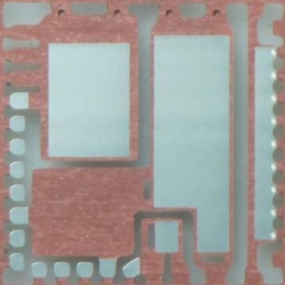
إطار الرصاص&الإطار المعدني لمصنع QFN, مادة إطار الرصاص هي C-194F.H, الطلاء الفضي على الرصاص(إطار معدني) أو طلاء الاتحاد الافريقي على LeadFrame(إطار معدني), نحن ننتج إطار QFN المعدني/إطار الرصاص مع جودة عالية ووقت قيادة سريعة.
يعد LeadFrame مكونًا أساسيًا في عبوة الدوائر المتكاملة (المرحلية), خاصة في Quad Flat لا الرصاص (QFN) الحزم. كما الطلب على الالكترونيات الحديثة أصغر, أكثر كفاءة, وحلول التعبئة والتغليف فعالة من حيث التكلفة, أصبحت حزم QFN ذات شعبية كبيرة نظرًا لحجمها الصغير, الأداء الحراري الممتاز, والموثوقية الكهربائية. الإطار الرصاصي, المستخدمة في حزم QFN, يلعب دورًا حاسمًا في توصيل قالب أشباه الموصلات بالدوائر الخارجية مع توفير الدعم الميكانيكي وتبديد الحرارة. تستكشف هذه المقالة التصميم, وظيفة, وفوائد إطارات الرصاص في حزم QFN, بالإضافة إلى نظرة عامة على عملية التصنيع.
ما هو الإطار الرئيسي?
الإطار الرصاصي عبارة عن هيكل معدني, عادة ما تكون مصنوعة من النحاس أو سبائك النحاس, مصممة لدعم وتوصيل قالب أشباه الموصلات كهربائيًا بالمكونات الخارجية. في حالة حزم QFN, يشكل الإطار الرئيسي الأساس الذي يدعم قالب IC ويوفر مسارات للإشارات الكهربائية. التصميم الفريد لتغليف QFN يزيل الخيوط البارزة, مع التوصيلات الكهربائية الموجودة أسفل العبوة. هذه الشقة, يؤدي التكوين الخالي من الرصاص إلى عامل شكل أصغر مقارنةً بالحزم التقليدية, مما يجعلها مثالية للتطبيقات ذات المساحة المحدودة.
دور Leadframe في حزم QFN
يؤدي الإطار الرئيسي في حزم QFN وظيفتين حيويتين: التوصيل الكهربائي والدعم الميكانيكي.
1. التوصيل الكهربائي
في حزمة QFN, يوفر الإطار الرئيسي الاتصال بين قالب IC والدوائر الخارجية. بعد أن يتم تركيب القالب على إطار الرصاص, يتم استخدام تقنيات ربط الأسلاك أو الرقاقة لتوصيل الوسادات الكهربائية للقالب بأسلاك إطار الرصاص. هذه الخيوط, توجد عادةً عند حواف وأسفل العبوة, الاتصال بلوحة الدوائر المطبوعة (ثنائي الفينيل متعدد الكلور) عندما يتم تركيب الحزمة. القصير, تصميم إطار الرصاص المسطح في QFN يقلل من الحث والمقاومة, مما يجعلها مناسبة للغاية للتطبيقات عالية السرعة وعالية التردد.
2. الدعم الميكانيكي والإدارة الحرارية
يوفر الإطار الرصاصي الاستقرار الميكانيكي أثناء عملية التجميع ويساعد على حماية IC أثناء التشغيل. بالإضافة إلى ذلك, اللوحة المكشوفة الموجودة أسفل حزمة QFN, وهو جزء من الرصاص, يسهل تبديد الحرارة بكفاءة. وهذا مهم بشكل خاص في التطبيقات التي تكون فيها الإدارة الحرارية أمرًا بالغ الأهمية, لأنه يسمح بنقل الحرارة مباشرة من القالب إلى PCB, منع ارتفاع درجة الحرارة وضمان التشغيل المستقر.
مزايا استخدام إطارات الرصاص في حزم QFN
توفر إطارات Leadframes العديد من المزايا في حزم QFN, مما يساهم في استخدامها على نطاق واسع في مختلف الصناعات:
- حجم صغير: حزم QFN صغيرة, خفيفة الوزن, ومنخفضة المستوى, مما يجعلها مثالية للتطبيقات حيث تكون المساحة محدودة, مثل الهواتف الذكية, الأجهزة القابلة للارتداء, وتطبيقات إنترنت الأشياء.
- أداء حراري ممتاز: توفر اللوحة المكشوفة للإطار الرصاصي في حزم QFN مسارًا حراريًا مباشرًا من IC إلى PCB, تحسين تبديد الحرارة وجعل الحزمة مناسبة لتطبيقات الطاقة العالية.
- فعالية التكلفة: يعد تصنيع إطار الرصاص عملية راسخة وفعالة من حيث التكلفة. إن بساطة تصميم QFN تقلل من استخدام المواد وتكاليف الإنتاج, مما يجعلها خيارًا ميسور التكلفة للإنتاج بكميات كبيرة.
- أداء كهربائي متفوق: توفر إطارات الرصاص في حزم QFN مقاومة منخفضة, التوصيلات الكهربائية ذات الحث المنخفض. وهذا يؤدي إلى تعزيز سلامة الإشارة, مما يجعل حزم QFN مثالية للتطبيقات التي تتطلب نقل بيانات عالي السرعة والحد الأدنى من فقدان الإشارة.
عملية تصنيع إطارات الرصاص لحزم QFN
يتضمن إنتاج إطارات الرصاص عادة إما ختم أو حفر ورقة رقيقة من النحاس أو سبائك النحاس في الشكل المطلوب. ثم يتم طلاء المعدن بمواد مثل الفضة, ذهب, أو البلاديوم لتعزيز التوصيل ومنع التآكل. بعد أن يتم تركيب قالب أشباه الموصلات على إطار الرصاص, يتم إجراء ربط الأسلاك أو ربط الرقاقة لتوصيل وسادات القالب بالوصلات. يتبع التغليف, حيث يتم تطبيق مركب القالب لحماية مجموعة IC وإطار الرصاص. تتضمن الخطوات النهائية تشذيب وتشكيل الخيوط لضمان التوصيلات الدقيقة مع لوحة PCB.
خاتمة
تعد إطارات الرصاص جزءًا لا يتجزأ من نجاح حزم QFN, تقديم توصيلات كهربائية موثوقة, الدعم الميكانيكي, وأداء حراري فائق في شكل مضغوط. مع استمرار الإلكترونيات في التقلص في الحجم وزيادة التعقيد, ستظل عبوات QFN القائمة على إطار الرصاص حلاً شائعًا وفعالاً من حيث التكلفة للتطبيقات عالية الأداء. مع قدرتها على تلبية متطلبات الأجهزة الإلكترونية الحديثة, تعد إطارات الرصاص جزءًا لا غنى عنه في صناعة تعبئة أشباه الموصلات.