minimum-spacing-pcb
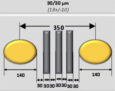
最小間隔の PCB 製造. Alcanta offer the Minimum Gap PCB boards. We have produced the smallest spacning pcb 回路基板. パッドとパッドの間の距離. we made them with 301つ(1.2ミル), 401つ(1.6ミル), 501つ(2.0ミル). 601つ, 701つ. ギャップ許容差は +/-10um.
For the processing capability of mainstream PCB manufacturers, the distance between the wires and the wires must be at least 4 ミル. The minimum line spacing is also the line-to-line, line-to-pad distance. From a production point of view, the larger the better, the more common is 6~8mil.

As far as the processing capability of mainstream PCB manufacturers is concerned, if the hole diameter of the pad is mechanically drilled, the minimum is not less than 0.15mm(6ミル). If laser drilling is used, the minimum is not less than 3mil. Most are 4mil via. The aperture tolerance is slightly different depending on the plate. 一般的に, the control can be within 0.05mm, and the pad width should be at least 0.2mm.
When we make the Minimum Spacing circuit board. we will use advanced production technology. the All smallest the pads to the pads spacing or the line to the line distance will be in the control. もちろん. You have to give us a Standard tolerance range. the Standard tolerance range is +/-10um. のように: the pads to pads spacing are 50um(2.0ミル). the finished the pads to the pads distance will be 40um to 60um. this is an example.

Our company offer the Minimum Spacing PCB from 2 レイヤーに 30 レイヤー. they are Mini LED PCB, リジッドフレックス & フレキシブル回路, 埋め込みビアおよびブラインドビア PCB, ハイブリッド & 混合誘電体 PCB, HDI PCB, Module PCB, 航空用基板, military PCB projects, High frequency communication PCB, その他.
ご質問がございましたら, お気軽にお問い合わせください info@alcantapcb.com , 喜んでお手伝いさせていただきます。
 アルカンタテクノロジー(深セン)株式会社