المحدودة")
أسلاك فائقة الكثافة ركائز الشركة المصنعة.كشركة مصنعة لركائز الأسلاك عالية الكثافة, نحن متخصصون في إنتاج ركائز متطورة تتيح أعلى مستويات التصغير والأداء في الأجهزة الإلكترونية. تضمن عمليات التصنيع المتقدمة لدينا سلامة الإشارة الفائقة والإدارة الحرارية, مما يجعل ركائزنا مثالية للتطبيقات في مجال الحوسبة عالية الأداء, الاتصالات السلكية واللاسلكية, والأجهزة الطبية. مع التركيز على الابتكار والجودة, نحن ملتزمون بتلبية الاحتياجات المتطورة لصناعة الإلكترونيات.
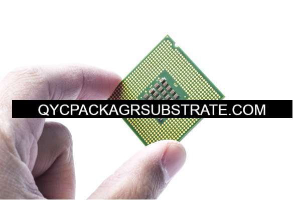
أسلاك فائقة الكثافة (UHDW) تعتبر الركائز عنصرًا حاسمًا في تطوير الأجهزة الإلكترونية المتقدمة. تم تصميم هذه الركائز لدعم الأسلاك الدقيقة للغاية والوصلات البينية عالية الكثافة, مما يجعلها ضرورية للتطبيقات التي تتطلب الأداء العالي والتصغير. تُستخدم ركائز UHDW في مجموعة متنوعة من المجالات, بما في ذلك أشباه الموصلات, الاتصالات السلكية واللاسلكية, والالكترونيات الاستهلاكية, تمكين إنشاء الاتفاق, قوي, والأجهزة الفعالة.
ما هي ركيزة الأسلاك عالية الكثافة للغاية?
أسلاك فائقة الكثافة (UHDW) الركيزة هي نوع من لوحات الدوائر المطبوعة (ثنائي الفينيل متعدد الكلور) الذي يتميز بأسلاك دقيقة للغاية وكثافة عالية من التوصيلات البينية. تم تصميم هذه الركائز لاستيعاب التعقيد المتزايد والتصغير للأجهزة الإلكترونية الحديثة. عادةً ما يتم تصنيع ركائز UHDW باستخدام مواد وعمليات تصنيع متقدمة لضمان قدرتها على دعم الإشارات عالية التردد, توزيع الطاقة, والإدارة الحرارية مع الحفاظ على عامل الشكل المضغوط.
الدليل المرجعي لتصميم الركيزة UHDW
يتضمن تصميم ركيزة UHDW عدة اعتبارات مهمة لضمان الأداء الأمثل. توضح الأقسام التالية الجوانب الرئيسية لتصميم الركيزة UHDW.
يعد اختيار المواد أمرًا بالغ الأهمية لأداء ركائز UHDW. تشمل المواد الرئيسية:
مواد الركيزة: مواد عالية الأداء مثل راتينج BT, ABF (فيلم بناء أجينوموتو), ويتم استخدام الركائز المملوءة بالسيراميك بشكل شائع نظرًا لخصائصها الكهربائية الممتازة وثباتها الحراري.
احباط النحاس: يتم استخدام النحاس عالي النقاء للآثار والطائرات الموصلة, توفير الموصلية الكهربائية الممتازة والموثوقية.
التحضير المسبق والتصفيح: يتم استخدام مواد مسبقة التحضير ومواد صفائحية عالية الأداء لربط الطبقات معًا, تقدم خسارة عازلة منخفضة والاستقرار الحراري العالي.
مواد لاصقة منخفضة الخسارة: مواد لاصقة متخصصة تحافظ على الأداء الكهربائي مع ربط الطبقات الرقيقة معًا.
تم تصميم طبقة المكدس لدعم متطلبات الأسلاك عالية الكثافة للركيزة مع الحفاظ على عامل الشكل المضغوط:
طبقات الإشارة: تُستخدم طبقات إشارة متعددة لتوجيه الإشارات عالية التردد. تم تصميم هذه الطبقات بممانعة يمكن التحكم فيها لضمان الحد الأدنى من فقدان الإشارة وسلامة الإشارة العالية.
طائرات الطاقة والأرضية: توفر الطاقة المخصصة والطائرات الأرضية مراجع جهد ثابتة وتقلل من الضوضاء, وهو أمر بالغ الأهمية للحفاظ على سلامة الإشارة في التطبيقات عالية التردد.
طبقات الإدارة الحرارية: طبقات إدارة حرارية رقيقة, مثل المنافذ الحرارية وموزعات الحرارة, يتم دمجها لتبديد الحرارة الناتجة عن المكونات عالية التردد, ضمان أداء موثوق.
ما هي المواد المستخدمة في ركائز UHDW?
يتم اختيار المواد المستخدمة في ركائز UHDW وفقًا لمواصفاتها الكهربائية, حراري, والخصائص الميكانيكية:
ركائز عالية الأداء: مواد مثل راتينج BT, ABF, ويتم استخدام الركائز المملوءة بالسيراميك نظرًا لخصائصها الكهربائية الممتازة وثباتها الحراري.
احباط النحاس: يتم استخدام النحاس عالي النقاء للآثار والطائرات الموصلة, توفير الموصلية الكهربائية الممتازة والموثوقية.
التحضير المسبق والتصفيح: يتم استخدام مواد مسبقة التحضير ومواد صفائحية عالية الأداء لربط الطبقات معًا, تقدم خسارة عازلة منخفضة والاستقرار الحراري العالي.
مواد لاصقة منخفضة الخسارة: مواد لاصقة متخصصة تحافظ على الأداء الكهربائي مع ربط الطبقات الرقيقة معًا.
ما هو حجم ركائز UHDW?
يختلف حجم ركائز UHDW وفقًا للتطبيق ومتطلبات التصميم المحددة:
سماكة: يمكن أن يتراوح سمك ركائز UHDW من أقل من 0.2 ملم إلى عدة ملليمترات, اعتمادًا على عدد الطبقات ومتطلبات الإدارة الحرارية.
أبعاد: يتم تحديد طول وعرض الركائز حسب حجم المكونات وتخطيط النظام. يمكن أن تتراوح من عوامل الشكل الصغيرة للأجهزة المدمجة إلى ركائز أكبر للأنظمة الإلكترونية المعقدة.
عملية تصنيع ركائز UHDW
تتضمن عملية تصنيع ركائز UHDW عدة خطوات دقيقة ومضبوطة لضمان الجودة والأداء العالي:
مواد الركيزة عالية الأداء, رقائق النحاس, المواد المسبقة, ويتم تحضير المواد اللاصقة وتقطيعها إلى أحجام مناسبة للمعالجة.
يتم تصنيع الطبقات عن طريق تصفيح المواد الموصلة والعازلة في كومة. تم تصميم كل طبقة باستخدام الطباعة الحجرية الضوئية لتحديد الدوائر المعقدة.
يتم حفر الميكروفياس والثقوب باستخدام تقنيات الحفر بالليزر أو الميكانيكية. ثم يتم طلاء هذه الثقوب بالنحاس لإنشاء توصيلات كهربائية بين الطبقات.
يتم تصفيح الطبقات الفردية معًا تحت الحرارة والضغط لتكوين مادة صلبة, هيكل متعدد الطبقات. تضمن هذه العملية ربط جميع الطبقات ومحاذاةها بقوة.
تُستخدم عمليات الطباعة الحجرية الضوئية والحفر لإنشاء دوائر دقيقة على كل طبقة, تتطلب دقة عالية للتوصيل الدقيق.
بعد التصنيع, يتم تجميع اللوحة بأي مكونات وموصلات ضرورية. يتم إجراء اختبارات صارمة للتأكد من أن اللوحة تلبي جميع مواصفات التصميم ومتطلبات الأداء.
مجال تطبيق ركائز UHDW
تُستخدم ركائز UHDW في نطاق واسع من التطبيقات عالية الأداء:
في تطبيقات أشباه الموصلات, تُستخدم ركائز UHDW لإنشاء اتصالات بينية عالية الكثافة بين الدوائر المتكاملة, تمكين تطوير المعالجات الدقيقة المتقدمة, رقائق الذاكرة, وغيرها من أجهزة أشباه الموصلات.
في الاتصالات السلكية واللاسلكية, تُستخدم ركائز UHDW في المحطات الأساسية, هوائيات, وغيرها من معدات الاتصالات عالية التردد لضمان نقل واستقبال الإشارة بشكل موثوق.
في الالكترونيات الاستهلاكية, ركائز UHDW تمكن من تطوير المدمجة, الأجهزة عالية الأداء مثل الهواتف الذكية, أقراص, والأجهزة القابلة للارتداء, حيث تكون المساحة أعلى من قيمتها.
في الأجهزة الطبية, تُستخدم ركائز UHDW في أنظمة التصوير, معدات التشخيص, وأجهزة الاتصال اللاسلكية, حيث يكون الأداء عالي التردد أمرًا ضروريًا.
في صناعة السيارات, تُستخدم ركائز UHDW في أنظمة مساعدة السائق المتقدمة (ADAS), أنظمة المعلومات والترفيه, وغيرها من وحدات التحكم الإلكترونية (وحدات التحكم الإلكترونية) التي تتطلب معالجة إشارات عالية التردد في شكل مضغوط.
ما هي مزايا ركائز UHDW?
توفر ركائز UHDW العديد من المزايا التي تجعلها لا غنى عنها في التطبيقات عالية الأداء:
تصميم مدمج: يسمح شكلها الرفيع بالاندماج في الأجهزة الإلكترونية المدمجة, توفير المساحة وتقليل الوزن.
أداء عالي: أنها توفر خصائص كهربائية ممتازة, مما يتيح نقل إشارة موثوقة عالية التردد بأقل قدر من الخسارة.
سلامة الإشارة: يتم الحفاظ على سلامة الإشارة العالية من خلال المعاوقة الخاضعة للرقابة والمواد منخفضة الخسارة, ضمان نقل إشارة دقيقة.
الإدارة الحرارية: تمنع تقنيات الإدارة الحرارية الفعالة ارتفاع درجة الحرارة وتضمن الأداء المتسق.
الاستقرار الميكانيكي: على الرغم من ملفهم الشخصي رقيقة, توفر هذه الركائز دعمًا ميكانيكيًا قويًا لتحمل ضغوط المناولة والتشغيل في البيئات عالية التردد.
مصداقية: تضمن المواد عالية الجودة وعمليات التصنيع الدقيقة الموثوقية والأداء على المدى الطويل.
التعليمات
ما هي الاعتبارات الأساسية في تصميم الركيزة UHDW?
وتشمل الاعتبارات الرئيسية اختيار المواد للأداء الكهربائي والحراري, تكديس الطبقات للتوجيه المعقد, سلامة الإشارة, توزيع الطاقة, الإدارة الحرارية, الاستقرار الميكانيكي, والموثوقية.
كيف تختلف ركائز UHDW عن الركائز القياسية عالية الكثافة?
تم تصميم ركائز UHDW خصيصًا لتوفير أسلاك دقيقة للغاية واتصالات بينية عالية الكثافة, في حين أن الركائز القياسية عالية الكثافة قد لا تحقق نفس المستوى من التصغير والأداء. تعتبر ركائز UHDW مثالية للتطبيقات التي تكون فيها المساحة والأداء أمرًا بالغ الأهمية.
ما هي عملية التصنيع النموذجية لركائز UHDW؟?
تتضمن العملية إعداد المواد, تصنيع الطبقة, الحفر والطلاء, التصفيح, نمذجة الدوائر, حَشد, واختبارات صارمة لضمان الجودة والأداء العالي.
ما هي التطبيقات الرئيسية لركائز UHDW?
تُستخدم ركائز UHDW في أشباه الموصلات, الاتصالات السلكية واللاسلكية, الالكترونيات الاستهلاكية, الأجهزة الطبية, وتطبيقات السيارات, توفير وظائف متقدمة وموثوقية في بيئات عالية الأداء.