المحدودة")
متعدد الطبقات للغاية ركائز FC-BGA الشركة المصنعة.كشركة مصنعة متقدمة لركائز FC-BGA متعددة الطبقات, نحن متخصصون في إنتاج حلول التوصيل البيني عالية الكثافة للتطبيقات الإلكترونية المتطورة. توفر ركائزنا أداءً استثنائيًا, الإدارة الحرارية, وسلامة الإشارة, مما يجعلها مثالية للحوسبة عالية الأداء, الاتصالات السلكية واللاسلكية, ومراكز البيانات. مع أحدث عمليات التصنيع ومراقبة الجودة الصارمة, نحن نضمن أن منتجاتنا تلبي أعلى معايير الصناعة, تقديم الموثوقية والابتكار لعملائنا.
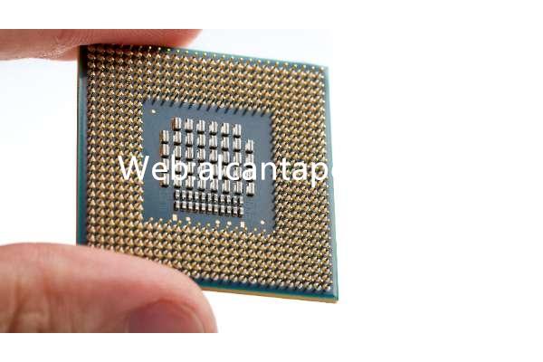
متعدد الطبقات للغاية FC-BGA (مصفوفة شبكة كرة الوجه ذات الرقاقة) ركائز هي لوحات دوائر متطورة تستخدم في تعبئة أشباه الموصلات لتعزيز الاتصال والأداء للدوائر المتكاملة (المرحلية) والمعالجات الدقيقة. تلعب هذه الركائز دورًا حاسمًا في الإلكترونيات الحديثة من خلال توفير منصة قوية للتوصيلات البينية عالية الكثافة وتبديد الحرارة بكفاءة. توفر هذه المقالة استكشافًا متعمقًا لركائز FC-BGA متعددة الطبقات للغاية, تفصيل تكوينها, عملية التصنيع, التطبيقات, والمزايا.
ما هي ركائز FC-BGA فائقة التعددية؟?
ركائز FC-BGA متعددة الطبقات للغاية عبارة عن لوحات دوائر متقدمة مصممة بطبقات متعددة من المواد الموصلة والعازلة, مما يسمح بالتوصيل البيني الكثيف لأجهزة أشباه الموصلات باستخدام تقنية رقاقة الوجه. تتميز هذه الركائز عادةً بمصفوفة شبكية كروية (بغا) إعدادات, حيث تعمل كرات اللحام الموجودة على الجانب السفلي من الركيزة على تسهيل التوصيلات الكهربائية بلوحة الدوائر المطبوعة (ثنائي الفينيل متعدد الكلور) أو ركيزة أخرى. تتميز ركائز FC-BGA متعددة الطبقات بعدد طبقاتها العالي, وصلات الملعب الدقيقة, وقدرات الإدارة الحرارية المتقدمة.
هيكل ركائز FC-BGA متعددة الطبقات
تم تصميم هيكل ركائز FC-BGA متعددة الطبقات للغاية لتحقيق أقصى قدر من الأداء الكهربائي, تبديد حراري, والاستقرار الميكانيكي. وتشمل العناصر الهيكلية الرئيسية:
عادة ما تكون مصنوعة من مواد عالية الأداء مثل شرائح الايبوكسي (على سبيل المثال, FR-4), بوليميدات, أو السيراميك المتقدم (على سبيل المثال, الألومينا أو نيتريد الألومنيوم). يعتمد اختيار مادة الركيزة على متطلبات التطبيق المحددة للخصائص الكهربائية, الموصلية الحرارية, والقوة الميكانيكية.
يتكون من طبقات متعددة متناوبة من الآثار الموصلة (النحاس أو المعادن الأخرى) والمواد العازلة (الراتنج أو الايبوكسي المقوى بالزجاج). يتيح المكدس متعدد الطبقات التوجيه المعقد للإشارات الكهربائية وتوزيع الطاقة, دعم نقل البيانات عالي السرعة وتقليل فقدان الإشارة.
أجهزة أشباه الموصلات (المرحلية أو المعالجات الدقيقة) يتم تركيبها مباشرة على الركيزة باستخدام تقنية رقاقة الوجه, حيث تقوم نتوءات اللحام بتوصيل وسادات ربط الشريحة بالوسادات المقابلة الموجودة على الركيزة. هذا التكوين يقلل من السعة الطفيلية والحث, تعزيز الأداء الكهربائي.
ثقوب صغيرة (فيا) وmicrovias يتم حفرها من خلال طبقات الركيزة ومليئة بالمواد الموصلة (على سبيل المثال, نحاس) لإنشاء اتصالات كهربائية عمودية بين طبقات مختلفة من الركيزة. تعد Microvias ضرورية لتحقيق اتصالات بينية عالية الكثافة مع درجة حرارة جيدة وتقليل تأخير انتشار الإشارة.
طبقة واقية تطبق على سطح الركيزة, باستثناء المناطق التي يتم فيها إجراء اتصالات اللحام. يعمل قناع اللحام على تحسين موثوقية وصلة اللحام, يمنع الجسور اللحام, ويحمي من العوامل البيئية.
يتميز الجانب السفلي من الركيزة بكرات لحام مرتبة في نمط شبكي (تكوين بغا). تعمل كرات اللحام هذه كاتصالات كهربائية لتركيب الركيزة على ثنائي الفينيل متعدد الكلور أو أي ركيزة أخرى, ضمان التوصيلات الكهربائية والميكانيكية الموثوقة.
المواد المستخدمة في ركائز FC-BGA متعددة الطبقات للغاية
تستخدم ركائز FC-BGA متعددة الطبقات للغاية مواد متقدمة تم اختيارها لكهربائها, حراري, والخصائص الميكانيكية, مصممة لتلبية متطلبات الأداء للتطبيقات عالية السرعة وعالية التردد. تشمل المواد الرئيسية:
وتشمل الخيارات شرائح على أساس الايبوكسي (على سبيل المثال, FR-4), بوليميدات (على سبيل المثال, الكابتن), أو السيراميك المتقدم (على سبيل المثال, الألومينا أو نيتريد الألومنيوم). توفر هذه المواد مجموعات مختلفة من العزل الكهربائي, الموصلية الحرارية, والقوة الميكانيكية لتناسب احتياجات التطبيقات المتنوعة.
النحاس هو المادة الأساسية المستخدمة في الخطوط الموصلة وطائرات الطاقة نظرًا لتوصيله الكهربائي الممتاز وموثوقيته في الدوائر عالية التردد. يمكن استخدام طبقات رقيقة من الذهب أو المعادن النبيلة الأخرى في تطبيقات محددة تتطلب مقاومة فائقة للتآكل أو موثوقية الاتصال الكهربائي.
المواد القائمة على الراتنج (على سبيل المثال, الايبوكسي أو بوليميد) أو يتم استخدام شرائح الإيبوكسي المقواة بالزجاج كطبقات عازلة لتوفير العزل الكهربائي بين الآثار والطبقات الموصلة. توفر هذه المواد ثوابت عازلة منخفضة وخصائص مقاومة يمكن التحكم فيها لنقل الإشارات بسرعة عالية.
سبائك لحام خالية من الرصاص (على سبيل المثال, SAC305) تستخدم عادة لكرات اللحام والوصلات البينية, الامتثال للوائح البيئية وضمان التوصيلات الميكانيكية والكهربائية القوية.
تشمل الخيارات المواد الحافظة العضوية القابلة للحام (OSP), القصدير الغمر (إمسن), أو الذهب الغمر بالنيكل اللاكهربائي (يوافق), يتم تطبيقه على سطح الركيزة لتعزيز موثوقية وصلة اللحام, منع الأكسدة, وتحسين أداء الاتصال الكهربائي.
عملية تصنيع ركائز FC-BGA متعددة الطبقات للغاية
تتضمن عملية تصنيع ركائز FC-BGA متعددة الطبقات للغاية تقنيات متقدمة وهندسة دقيقة لتحقيق اتصالات بينية عالية الكثافة, الأداء الكهربائي الأمثل, والموثوقية. تتضمن العملية عادة الخطوات التالية:
يقوم المهندسون بتصميم تخطيط الركيزة باستخدام التصميم بمساعدة الكمبيوتر (CAD) برمجة, تحديد موضع أجهزة أشباه الموصلات, آثار موصلة, فيا, وكرات اللحام.
مادة الركيزة الأساسية (على سبيل المثال, صفح على أساس الايبوكسي أو السيراميك) يتم تحضيرها وتقطيعها إلى ألواح ذات حجم مناسب. تقنيات تحضير السطح, مثل التنظيف وتخشين السطح, يتم استخدامها لتعزيز التصاق الطبقات اللاحقة.
طبقات بديلة من رقائق النحاس الموصلة والتجهيزات العازلة (قطعة قماش زجاجية مشربة بالراتنج) أو يتم تكديس المواد الأساسية لتكوين مجموعة متعددة الطبقات. يتم بعد ذلك ضغط المكدس وتسخينه في مكبس تصفيح لربط الطبقات معًا, تشكيل الركيزة المركبة الصلبة.
يتم استخدام معدات الحفر الدقيقة لإنشاء ثقوب للمنافذ والميكروفياس من خلال المكدس متعدد الطبقات. يتم استخدام تقنيات الحفر بالليزر أو الحفر الميكانيكي, اعتمادا على حجم وكثافة متطلبات فيا.
يتم طلاء Vias وmicrovias بمادة موصلة (عادة النحاس) لإنشاء اتصالات كهربائية بين طبقات مختلفة من الركيزة. يتبع طلاء النحاس ترسب طبقة رقيقة من المعدن النبيل (على سبيل المثال, ذهب) على الأسطح المكشوفة لتعزيز قابلية اللحام ومنع الأكسدة.
يتم حفر رقائق النحاس الموصلة على الطبقات الخارجية للركيزة باستخدام العمليات الكيميائية أو الطباعة الحجرية الضوئية لتحديد آثار الدائرة, منصات, ومسارات الإشارة حسب المواصفات التصميمية.
طبقات رقيقة من المعادن الموصلة (على سبيل المثال, الذهب أو النيكل) يتم ترسيبها على سطح الركيزة باستخدام تقنيات مثل الرش أو الطلاء الكهربائي لإنشاء أسطح قابلة للحام وضمان اتصالات كهربائية موثوقة. مواد تشطيب السطح (على سبيل المثال, OSP, يوافق) يتم تطبيقها لحماية الأسطح المعدنية المكشوفة وتحسين جودة وصلة اللحام.
يتم وضع كرات اللحام بدقة وربطها بالجانب السفلي من الركيزة باستخدام عمليات التوزيع الآلي وإعادة التدفق. تشكل كرات اللحام مصفوفة شبكية كروية (بغا) إعدادات, توفير اتصالات كهربائية لتركيب الركيزة على PCB أو ركيزة أخرى.
تخضع ركائز FC-BGA المجمعة متعددة الطبقات لعمليات اختبار وفحص صارمة للتحقق من الاستمرارية الكهربائية, التحكم في المعاوقة, سلامة مشتركة لحام, والوظيفة الشاملة. تشمل الاختبارات الاختبارات الكهربائية, ركوب الدراجات الحرارية, فحص الأشعة السينية, والفحص البصري الآلي (الهيئة العربية للتصنيع) للكشف عن العيوب وضمان ضمان الجودة.
مجالات تطبيق ركائز FC-BGA متعددة الطبقات
تجد ركائز FC-BGA متعددة الطبقات استخدامًا واسع النطاق في التطبيقات الإلكترونية المتقدمة التي تتطلب توصيلات بينية عالية الكثافة, أداء كهربائي متفوق, وإدارة حرارية موثوقة. وتشمل مجالات التطبيق الرئيسية:
تستخدم في الخوادم, أجهزة الكمبيوتر العملاقة, ومراكز البيانات لدعم معالجة البيانات عالية السرعة, الذكاء الاصطناعي (منظمة العفو الدولية), وتطبيقات التعلم الآلي.
المنتشرة في أجهزة توجيه الشبكة, المفاتيح, ومعدات الاتصالات للتعامل مع الإشارات عالية التردد ونقل البيانات مع زمن وصول منخفض والحد الأدنى من فقدان الإشارة.
مدمجة في الهواتف الذكية, أقراص, والأجهزة القابلة للارتداء لدعم الوظائف المعقدة, شاشات عالية الدقة, وإدارة الطاقة بكفاءة.
تستخدم في أنظمة مساعدة السائق المتقدمة (ADAS), أنظمة المعلومات والترفيه, ووحدات التحكم في المركبات لضمان التشغيل الموثوق في بيئات السيارات القاسية.
تطبق في مجال الروبوتات, وحدات تحكم الأتمتة, وإنترنت الأشياء الصناعي (إنترنت الأشياء) الأجهزة لتمكين التحكم في الوقت الحقيقي, يراقب, ومعالجة البيانات في التصنيع والبيئات الصناعية.
المستخدمة في معدات التصوير الطبي, أجهزة التشخيص, والإلكترونيات القابلة للزرع لتوفير تحكم دقيق, موثوقية عالية, والأداء طويل المدى في تطبيقات الرعاية الصحية.
مزايا ركائز FC-BGA فائقة متعددة الطبقات
توفر ركائز FC-BGA متعددة الطبقات العديد من المزايا التي تجعلها لا غنى عنها في التغليف الإلكتروني عالي الأداء:
يتيح التكديس متعدد الطبقات والميكروفيات الدقيقة التوجيه الكثيف للإشارات وتوزيع الطاقة, دعم التصاميم الإلكترونية المعقدة والتصغير.
تضمن السعة الطفيلية المنخفضة والمحاثة التي يتم تحقيقها من خلال الوصلات البينية لرقاقة الوجه وتقنيات التوجيه المتقدمة نقل الإشارة بسرعة عالية, انخفاض تأخير الإشارة, والحد الأدنى من التداخل الكهرومغناطيسي (إيمي).
المنافذ الحرارية المتقدمة, بالوعة الحرارة, وتقنيات التبديد الحراري بشكل فعال
تبديد الحرارة الناتجة عن أجهزة أشباه الموصلات عالية الطاقة, الحفاظ على درجات حرارة التشغيل المثلى وإطالة عمر المكونات.
بناء قوي, وصلات لحام موثوقة, وتضمن إجراءات الاختبار الصارمة الموثوقية على المدى الطويل, الاستقرار الميكانيكي, ومقاومة العوامل البيئية مثل تقلبات درجات الحرارة والاهتزازات.
دعم للمواد الركيزة المتنوعة, التشطيبات السطحية, وتتيح تقنيات التجميع إمكانية التخصيص وفقًا لمتطلبات التطبيق المحددة, تسهيل الابتكار وتمييز المنتجات.
التعليمات
كيف تعمل ركائز FC-BGA متعددة الطبقات على تسهيل نقل الإشارات عالي السرعة?
تحقق ركائز FC-BGA متعددة الطبقات للغاية نقل إشارة عالي السرعة من خلال تقنيات التوجيه المتقدمة, ميكروفياس الملعب غرامة, والمواد العازلة منخفضة, التقليل من تأخير انتشار الإشارة, عدم تطابق المعاوقة, والتداخل الكهرومغناطيسي (إيمي).
ما هي المزايا الرئيسية لاستخدام تقنية شرائح الوجه في ركائز FC-BGA متعددة الطبقات للغاية?**
تقنية رقاقة الوجه تلغي الحاجة إلى ربط الأسلاك, تقليل السعة الطفيلية والمحاثة مع تعزيز الأداء الكهربائي. كما أنه يتيح التوصيلات الحرارية والكهربائية المباشرة بين أجهزة أشباه الموصلات والركيزة, تحسين تبديد الحرارة وسلامة الإشارة.
في أي الصناعات تكون ركائز FC-BGA متعددة الطبقات للغاية هي الأكثر استخدامًا?
تُستخدم ركائز FC-BGA متعددة الطبقات للغاية في الغالب في صناعات مثل الحوسبة عالية الأداء, الاتصالات السلكية واللاسلكية, الالكترونيات الاستهلاكية, إلكترونيات السيارات, الأتمتة الصناعية, والأجهزة الطبية. تتطلب هذه الصناعات حلول تغليف متقدمة قادرة على دعم الوظائف المعقدة, موثوقية عالية, والأداء الفعال.
كيف يتم تصنيع ركائز FC-BGA متعددة الطبقات للغاية لضمان الموثوقية والجودة?
تخضع ركائز FC-BGA متعددة الطبقات للغاية لعملية تصنيع دقيقة تتضمن تصنيع الركيزة, تكديس الطبقة, حفر, المعادن, التشطيب السطحي, مرفق كرة اللحام, واختبار صارم. يتم التحكم في كل خطوة بعناية لتحقيق دقة الأبعاد الدقيقة, الأداء الكهربائي الأمثل, والسلامة الميكانيكية القوية, تلبية المتطلبات الصارمة للتطبيقات الإلكترونية عالية الأداء.